
High-speed digital signals and radio-frequency circuits do not forgive manufacturing imperfections. A 50-ohm transmission line that measures 52 ohms in production can reflect enough energy to corrupt a 10 Gbps data stream. A microvia with excessive stub length can turn a clean 5G antenna feed into a radiator of spurious emissions. At Keepbest, we assemble high-speed and RF boards for data center switches, 5G base stations, satellite communication payloads, and automotive radar modules. The manufacturing discipline required for these applications goes far beyond standard PCBA assembly.
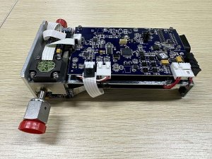
This guide explains what makes high-speed and RF assembly different, what process controls are essential, and how to qualify a manufacturer for your signal-integrity-critical design.
What Makes High-Speed and RF PCBA Different?
Standard PCBA assembly focuses on electrical continuity and solder joint reliability. High-speed and RF assembly adds a third dimension: controlled electromagnetic behavior.
Impedance Control: Transmission lines must maintain characteristic impedance within tight tolerances, typically plus or minus 5% or better. Deviations caused by trace width variation, dielectric thickness inconsistency, or copper roughness create reflections that degrade signal quality.
Signal Integrity: Rise times below 100 picoseconds behave like microwave signals even at relatively low clock frequencies. Crosstalk, ground bounce, and power supply noise become first-order design concerns that manufacturing variation can amplify or suppress.
EMI and EMC: Unintended radiation from imperfect grounds, via stubs, or unterminated traces can fail regulatory emission limits. The manufacturing process must preserve the designer’s EMC strategy.
Material Sensitivity: High-frequency substrates such as Rogers RO4350, Taconic TLY-5, or Panasonic Megtron 6 have different handling, drilling, and plating characteristics than standard FR-4. Process parameters must be adjusted accordingly.
Substrate and Layer Stack-Up Control
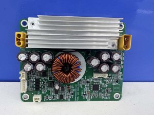
The foundation of signal integrity is the PCB fabrication process. Your manufacturing partner works with qualified fabrication partners who specialize in high-frequency materials.
| Parameter | Standard FR-4 | High-Frequency Material | Control Method |
| Dielectric constant tolerance | Plus or minus 10% | Plus or minus 2% | Material certification per lot |
| Trace width tolerance | Plus or minus 20 microns | Plus or minus 10 microns | Laser direct imaging |
| Dielectric thickness | Plus or minus 10% | Plus or minus 5% | In-process micrometer measurement |
| Copper roughness | 3-5 microns Rz | Less than 2 microns Rz | Reverse-treated foil or VLP copper |
Layer Stack-Up Verification: For multilayer boards with controlled impedance, the actual layer spacing is measured on coupons and compared against design values before assembly begins. Deviations trigger stack-up recalculation and trace width compensation.
Solder Paste and Reflow Considerations
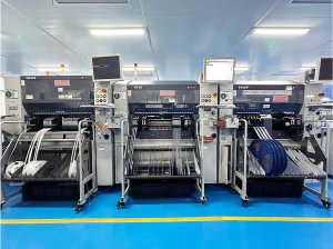
High-frequency components often use smaller packages with tighter pitches, requiring thinner stencils and more precise paste deposits.
Stencil Design: Stencil thickness is typically 100 microns for micro-BGA and CSP devices. Area ratios below 0.66 are avoided. Electropolished stencil apertures improve paste release for small openings.
Component Placement: Placement accuracy requirements tighten for high-speed designs. A 0201 capacitor placed 50 microns off-center may not affect a low-speed circuit, but the same misplacement on a 0402 RF termination resistor can shift impedance matching.
Reflow Profile: Lead-free SAC305 profiles must account for the thermal mass of dense high-layer-count boards. Excessive peak temperature can degrade high-frequency substrate properties. Insufficient peak temperature creates weak joints on large thermal pads.
Via and Interconnect Quality
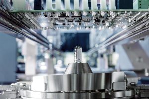
Vias are not just holes. In high-speed designs, they are transmission line discontinuities that must be carefully controlled.
Via Stub Management: Unused via barrel length below a signal layer creates a resonant stub. For high-speed designs, back-drilling removes the unused portion, reducing stub length to less than 10 mils.
Via Filling: Thermal vias beneath high-power RF amplifiers are often filled with conductive epoxy and plated over to provide both thermal and electrical continuity. Void-free filling is essential for consistent performance.
Microvia Reliability: HDI boards with laser-drilled microvias require plating quality verification. The EMS provider verifies microvia copper thickness and aspect ratio compliance before assembly.
Testing and Validation for High-Speed Designs
Standard ICT and FCT are necessary but not sufficient for high-speed boards.
Impedance Testing: Time-domain reflectometry (TDR) measures actual transmission line impedance on production boards. Results are compared against simulation models and design targets.
Network Analysis: Vector network analyzers measure S-parameters for RF circuits, verifying filter response, antenna matching, and amplifier gain across the operating frequency range.
Eye Diagram Analysis: For digital high-speed interfaces such as PCIe, USB 3.0, and 10GbE, eye diagram testing verifies that signal quality meets the specification mask under worst-case conditions.
EMI Pre-Compliance: Radiated and conducted emission scans identify unexpected radiation sources before formal compliance testing. This catches manufacturing-induced EMI issues such as insufficient ground stitching or floating shields.
Common High-Speed Manufacturing Defects
| Defect | Signal Integrity Impact | Our assembly team Prevention |
| Trace width variation | Impedance mismatch, reflections | Laser direct imaging, 100% coupon verification |
| Excessive via stub | Resonance, insertion loss | Back-drilling specification, X-section validation |
| Solder void in thermal via | Increased junction temperature | Vacuum-assisted filling, X-ray verification |
| Misplaced RF termination | Impedance mismatch, power reflection | Sub-35 micron placement, AOI with package recognition |
| Flux residue near RF traces | Dielectric constant change, detuning | Controlled cleaning, ion chromatography verification |
Design for Manufacturability for High-Speed PCBA
Manufacturing precision begins at the design stage.
Test Point Access: High-speed signals cannot be probed with standard ICT spring pins without degrading signal integrity. Design in dedicated test couplers, loopback paths, or boundary-scan access for manufacturing test.
Component Orientation: RF components such as couplers, filters, and amplifiers often have directional pinouts. Clear polarity indicators and consistent orientation reduce placement errors.
Thermal Management: High-speed circuits generate significant heat. Ensure thermal vias, heat sinks, and airflow paths are compatible with assembly tooling and inspection access.
Shielding Strategy: Metal shields over sensitive RF sections must be designed with adequate clearance for placement nozzles and inspection cameras. Snap-on shields may be preferred over soldered shields for serviceability.
Frequently Asked Questions
Q: What is the minimum frequency where high-speed manufacturing considerations apply?
As a rule of thumb, rise times below 1 nanosecond or clock frequencies above 500 MHz warrant high-speed manufacturing discipline. For RF, any design above 1 GHz requires controlled impedance and EMI-conscious assembly.
Q: Can standard FR-4 be used for high-speed designs?
For moderate speeds up to several gigahertz, high-quality FR-4 with tight dielectric tolerance may suffice. For multi-gigabit serial links or RF above 3 GHz, dedicated low-loss materials such as Rogers or Megtron are strongly recommended.
Q: How much does high-speed assembly cost compared to standard PCBA?
Expect a 20% to 50% premium depending on material cost, inspection depth, and test requirements. The premium is justified by the cost of field failures in high-speed systems, which can exceed the assembly cost by orders of magnitude.
Q: What test data should I request for high-speed production lots?
Impedance test reports from TDR measurements, S-parameter plots for RF circuits, eye diagram captures for digital interfaces, and EMI pre-compliance scan results. Keepbest provides all of these upon customer request.
Q: Does A qualified PCBA supplier support mmWave frequencies?
Yes. We have assembled boards operating at 24 GHz, 60 GHz, and 77 GHz for automotive radar, 5G mmWave, and satellite communication applications. These builds require specialized handling, ultra-clean environments, and precision placement.
Q: How early should a high-speed manufacturer be engaged in the design process?
As early as schematic capture. Manufacturing constraints on layer stack-up, via structures, and component availability directly impact signal integrity. The production partner offers pre-layout consulting to help designers avoid manufacturability pitfalls.
Building a high-speed or RF product? Send your stack-up, simulation models, and design files to the Keepbest high-speed engineering team. We will review your design for manufacturability, propose process controls, and provide a detailed quote for precision assembly.
