
PCB layout design transforms schematic diagrams into physical circuit boards, requiring a comprehensive consideration of circuit performance, electromagnetic compatibility, thermal management and manufacturing processes. This article analyses the key impacts of layout design on electrical performance, manufacturability and cost efficiency, and outlines the core design process.
1.The Value of Optimising Electrical Performance
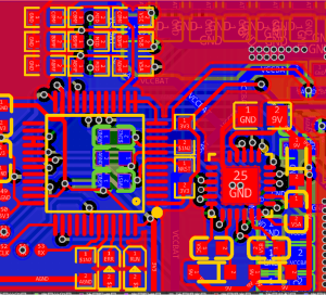
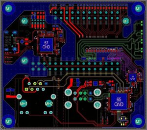
A well-designed layout can shorten high-frequency signal paths and prevent electromagnetic interference and signal crosstalk. BGA-packaged components require precise blind and buried via routing techniques to achieve high-density connections and ensure signal integrity.
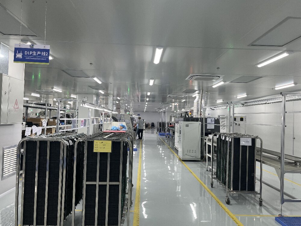
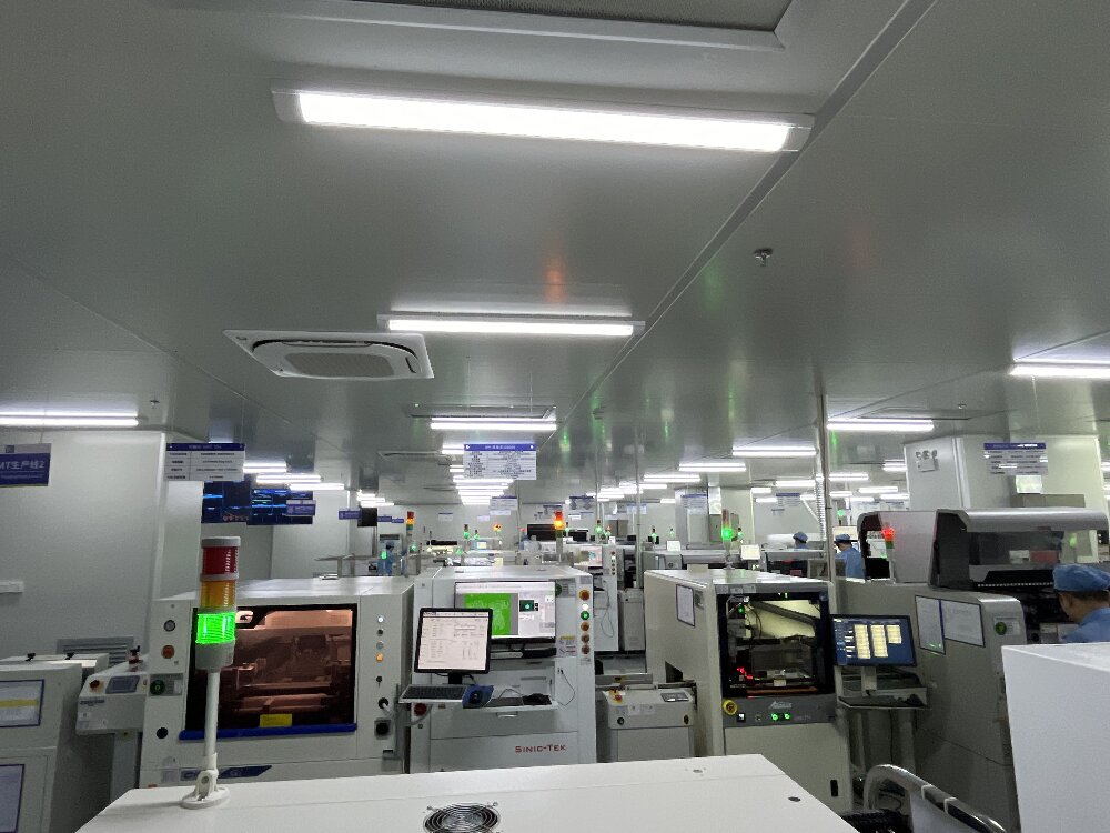
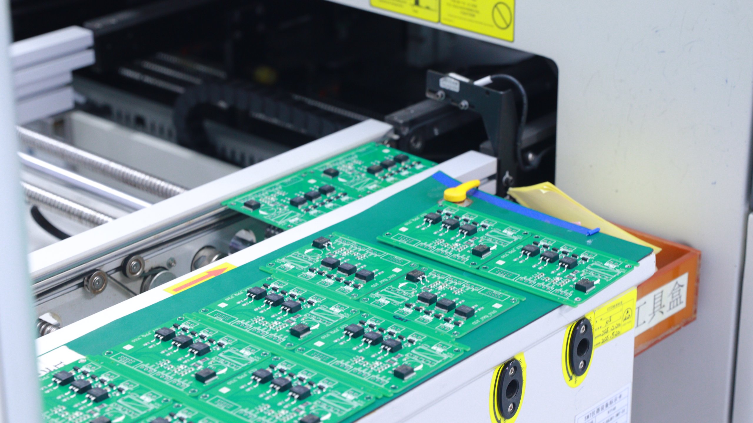
2.Ensuring Manufacturability
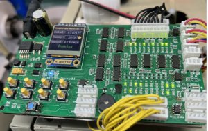
The design must align with manufacturing processes, including the definition of parameters such as pad dimensions and via diameters. A standardised layout can prevent issues such as warping and cold solder joints during production, thereby improving first-pass yield.
3. Strategies for Balancing Cost and Efficiency
By optimising the number of layers, reducing the number of vias, and rationally planning component placement, PCB material costs and assembly complexity can be reduced. Scientific layout and routing are the key to achieving the best value for money.
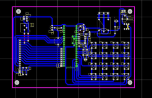
4.Core PCB Layout Processes
Component Placement: Arrange components according to signal flow and thermal management requirements, separating digital and analogue modules.
Rule Definition: Set parameters such as trace width, spacing and via diameter to ensure compliance with signal integrity and safety standards.
Routing Planning: Prioritise high-speed signal lines such as differential pairs and DDR, employing serpentine routing or impedance matching.
Post-Design Verification: Identify potential issues through design rule checks and simulation tools.