

Understanding Common SMT Component Packages Improves PCB Assembly Decisions
Choosing the correct SMT component package is one of the earliest and most consequential decisions an electronics designer makes, because the package chosen directly shapes every downstream step of PCB assembly. A surface-mount package defines pad geometry, stencil aperture, reflow behavior, inspection method, and rework strategy. When the SMT component package matches the product’s electrical, thermal, and volume requirements, PCB assembly runs smoothly with high first-pass yield. When it does not, manufacturers face tombstoning, solder voids, head-in-pillow defects, and costly rework.

The modern surface-mount landscape spans leaded parts such as SOIC and QFP, leadless parts such as QFN and DFN, area-array parts such as BGA and CSP, and land-grid parts such as LGA. Each family behaves differently on the pick-and-place machine and on the reflow oven. A reliable PCB assembly process starts by mapping each device’s package to the capabilities of the line, the test equipment available, and the expected production volume.
The table below summarizes how the most common SMT component package families compare across the variables that matter most on the assembly floor.
| Package family | Typical pitch | Primary inspection | Rework difficulty | Best fit |
|---|---|---|---|---|
| SOIC / SOP | 1.27 mm | AOI + visual | Low | Legacy, cost-sensitive boards |
| QFP | 0.4-0.8 mm | AOI + visual | Medium | Microcontrollers, analog ICs |
| QFN / DFN | 0.4-0.65 mm | AOI + X-ray sample | High | RF, power, small footprint |
| BGA / CSP | 0.4-1.0 mm | X-ray mandatory | Very high | MPUs, FPGAs, memories |
| LGA | 0.5-1.0 mm | X-ray + electrical | Very high | Connectors, sensors, modules |
QFN and DFN Packages Demand Precise Solder Paste Printing in PCB Assembly
Quad-flat-no-lead and dual-flat-no-lead packages have become the default choice for RF, power, and space-constrained designs, but they place tight demands on the solder paste printing stage of PCB assembly. The exposed pad beneath a QFN must be printed with a carefully reduced aperture to avoid solder bubbling, while the perimeter lands need enough paste volume to form a sound fillet. A small deviation in stencil thickness or aperture design translates directly into open joints or bridging.
Because the side terminations sit flush with the package body, an automated optical inspection system can only verify the meniscus at the toe. For this reason, a disciplined SMT assembly line qualifies the QFN stencil and reflow profile together, then confirms joint quality with periodic cross-section or X-ray sampling. Selecting a QFN when the line lacks this control is a common cause of field returns.

BGA and CSP Packages Require X-Ray Inspection During SMT Assembly
Ball-grid-array and chip-scale packages move all connections to the underside, making the joints invisible to conventional optical inspection. This single fact reshapes the PCB assembly test plan: X-ray inspection becomes mandatory, not optional. A 2D X-ray reveals voids, bridging, and missing balls, while 3D X-ray or laminography can measure joint volume and coplanarity for the densest CSP devices.
The reward for accepting this complexity is extraordinary routing density and excellent thermal and electrical performance, which is why BGA and CSP dominate processors, FPGAs, and high-speed memory. The trade-off is rework: removing and replacing a BGA demands a hot-air station, precise temperature profiling, and often a bottom-side heater. A PCB assembly partner that invests in X-ray and BGA rework capability is essential when your design leans on area-array packages.

LGA Packages Challenge PCB Assembly With Hidden Solder Joints
Land-grid-array packages place bare pads on the bottom of the component and matching lands on the board, with no balls or leads to absorb placement tolerance. The result is a very flat, low-profile connection that is excellent for signal integrity but punishing for assembly yield. An LGA joint forms only if the pad coplanarity, paste height, and placement pressure are all correct, and any contamination causes a hidden open that escapes visual checks.
Because the joints are fully concealed, PCB assembly quality for LGA parts relies on a clean process, controlled paste deposit, and electrical test or X-ray verification. Designers should reserve LGA for applications where height and electrical performance justify the added process discipline, and should confirm that the chosen assembler maintains the cleanliness and inspection rigor the package requires.
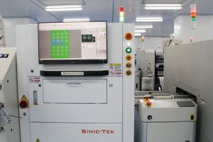
Leadless Packages Increase Rework Difficulty in PCB Assembly
Rework planning is frequently overlooked during package selection, yet it is where leadless and area-array parts impose the steepest penalty. A gull-wing SOIC can be lifted and replaced with a standard iron and modest skill, but a QFN, BGA, or LGA needs regulated hot air, a thermocouple-controlled profile, and often a preheater to avoid delaminating the board. The exposed thermal pad under a QFN further complicates removal because it welds the part to the board thermally.
A practical PCB assembly guideline is to reserve the most rework-hostile packages for the devices least likely to be wrong at first spin. Prototype builds benefit from larger, leaded packages that tolerate correction, while production transfers can adopt leadless parts once the design is frozen. Matching package difficulty to project maturity reduces scrap and speeds time to market.
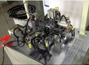
Thermal Performance of Component Packages Affects PCB Assembly Reliability
Every SMT component package conducts heat through a different path, and that path must be respected both in layout and in the assembly process. Power devices in QFN or DFN packages rely on the exposed pad soldered to a thermal land on the board; if that joint is starved of solder, junction temperature climbs and lifetime falls. Area-array packages spread heat through the balls into internal planes, which helps but also raises the stakes for void control under the die.
Selecting a package with adequate thermal resistance is only half the task; the PCB assembly process must deliver the intended thermal joint. This means correct paste volume on the exposed pad, sufficient via count in the thermal land, and a reflow profile that wets the pad fully. A package that is thermally ideal on paper can still fail in the field if assembly does not realize its thermal path.
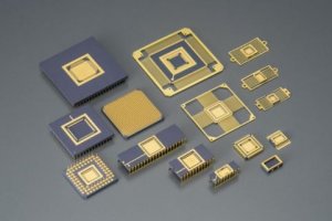
Package Pitch and Footprint Influence Automated Optical Inspection in SMT
As pitches shrink below 0.5 mm, the margin for paste misalignment and bridging collapses, and the effectiveness of automated optical inspection changes. Coarse-pitch leaded parts are easy for AOI to grade because the leads are visible and well separated. Fine-pitch QFN and dense BGA, by contrast, hide their critical joints, pushing inspection toward X-ray and toward functional test.
When selecting an SMT component package, weigh how the pitch affects your inspection strategy and cost. A part that forces X-ray on every unit is acceptable for high-value electronics but may be unnecessary for a simple consumer board. Balancing pitch, yield risk, and test cost is a core skill of good PCB assembly engineering, and it should inform the package shortlist from the first schematic.
- Evaluate the package against your line’s placement accuracy and stencil process.
- Confirm the inspection method the package requires is available and affordable.
- Estimate rework effort and reserve hostile packages for frozen designs.
- Check thermal path realization, not just the datasheet thermal rating.
- Verify component availability and moisture sensitivity before commitment.
Board Layout Must Match the Selected SMT Component Package for Assembly
The best package choice collapses if the printed circuit board layout does not support it. Footprint dimensions, solder-mask definition, thermal vias, and paste reduction must all follow the selected SMT component package’s recommended land pattern. A QFN with too little solder mask between pads invites bridging, while a BGA with insufficient via-in-pad filling traps air and creates voids during reflow.
Working with an experienced PCB assembly manufacturer during the footprint stage pays off here, because manufacturing feedback catches land-pattern errors before they reach a panel. A one-stop PCBA solution that reviews layout, stencil, and reflow together turns package selection from a isolated design choice into a verified, repeatable process. The right package and the right layout, decided together, are what keep first-pass yield high.

Summary
Selecting the right SMT component package is a foundational PCB assembly decision that determines yield, inspection cost, rework effort, and long-term reliability. Leadless and area-array packages such as QFN, BGA, CSP, and LGA deliver density and performance but demand X-ray inspection, disciplined paste printing, and careful thermal design. Matching each package to the production line’s capability and to the project’s maturity is the surest path to a clean, repeatable SMT assembly process.
FAQ
Which SMT component package is easiest to assemble and rework?
Leaded packages such as SOIC and QFP are the easiest, because their gull-wing leads are visible to optical inspection and can be reworked with a standard soldering iron. They suit prototypes and cost-sensitive boards where density is not the priority.
Why do BGA and CSP packages need X-ray inspection?
Their solder joints sit underneath the component and are invisible to cameras, so only X-ray can confirm voids, bridging, and ball coplanarity. Skipping X-ray on area-array packages risks shipping hidden open or weak joints.
Are QFN packages harder to assemble than QFP?
QFN parts are leadless with an exposed thermal pad, so they need precise stencil apertures and X-ray or cross-section verification, making them less forgiving than QFP. They reward the effort with a smaller footprint and better thermal performance.
How does package pitch affect PCB assembly cost?
Finer pitch raises placement accuracy requirements, increases bridging risk, and often forces X-ray or functional test, all of which add cost. Choosing the coarsest pitch that meets the design keeps inspection and yield costs down.
When should I avoid leadless packages in a new design?
Avoid them on early prototypes or designs likely to change, because rework is difficult and slow. Use leaded packages first to validate the circuit, then move to leadless parts once the layout is frozen for production.