
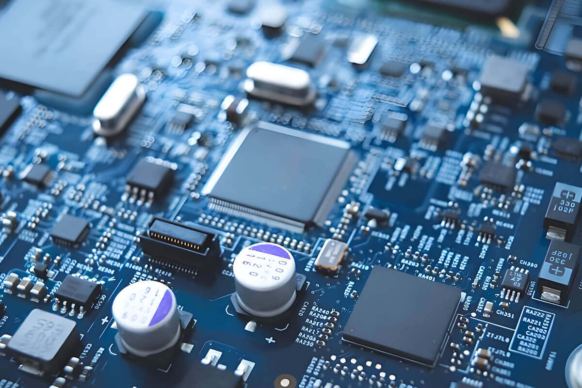
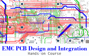
High-speed signal design presents a core challenge for communications equipment, servers and RF products. Signal integrity (SI) issues often only come to light during the PCB assembly stage, making debugging difficult. This article analyses the key rules of high-speed signal design from a layout perspective.
Definition and Impact of High-Speed Signals
Signals with a rise time of less than 1 ns or a frequency exceeding 100 MHz are generally considered high-speed signals.
Main issues: reflections, crosstalk, ground bounce and EMI radiation. These issues are directly related to the layout routing method.
Impedance Control Design
Characteristic impedance mismatch is the root cause of reflections.
Design considerations: Calculate the target impedance (commonly 50 Ω single-ended or 100 Ω differential), select appropriate trace widths, spacing and stack-up, confirm the dielectric constant (Dk) and board material tolerances with the PCB manufacturer, and reserve space for impedance test strips.
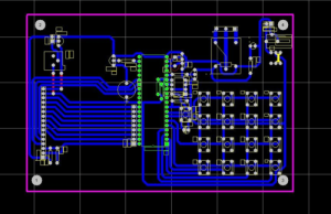
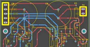
Trace Routing Rules for Differential Pairs
Differential signals (such as USB, HDMI and PCIe) require extremely high symmetry in trace routing.
Rules: Equal-length matching (typically <5 mil deviation), parallel spacing, avoidance of asymmetrical vias, and a continuous reference plane.
Return Paths and Ground Planes
The return current for high-speed signals flows directly beneath the signal traces.
Key principles: Avoid split planes, place ground vias as close as possible, ensure high-speed signal layers are adjacent to the reference plane, and minimise the inductance of the return path.
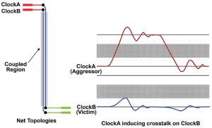
Crosstalk Control Strategies
Electromagnetic coupling between adjacent traces causes crosstalk.
Control methods: Increase trace spacing (3W rule), use striplines instead of microstrip lines, ground-wrap critical signals, and avoid long parallel traces.
EMC Pre-design
The cost of rectifying EMC issues at a later stage is extremely high.
Design techniques: filtering critical signals, shielding I/O ports, ground-wrapping clock lines, placing power decoupling capacitors in close proximity, and reserving space for shielding enclosures.
High-speed design requires consideration of manufacturing and test feasibility right from the layout stage. Confirm the high-speed board processing capabilities (e.g., impedance control accuracy of ±10%) with the PCB assembly factory to avoid a disconnect between design and process.
Frequently Asked Questions (FAQ)
Q1: What is the 3W rule?
A: The 3W rule stipulates that the centre-to-centre spacing between traces must be at least three times the trace width, in order to reduce crosstalk. For high-speed differential pairs or sensitive analogue signals, the 5W or 10W rule may sometimes be required, in conjunction with ground-wrapping.
Q2: What is the purpose of an impedance test coupon?
A test coupon is a dedicated test area manufactured alongside the PCB, used to measure actual impedance values. The factory uses a TDR (Time Domain Reflectometer) to verify that the impedance falls within ±10% of the target value. Test coupons are not used for product functionality; they are solely for process validation.
Q3: Can high-speed signals be routed to a different layer?
A: This should be avoided wherever possible. If it is necessary to route to a different layer, a ground via must be placed adjacent to the signal via to ensure a continuous return path. When routing differential pairs to a different layer, both signal lines must be routed to the same new layer whilst maintaining symmetry.
Q4: What is ground bounce?
A: High-speed switching currents cause localised voltage fluctuations on the ground plane. This manifests as an unstable signal reference level, leading to logic errors. Mitigation methods include adding decoupling capacitors, optimising the power distribution network (PDN), and reducing simultaneous switching noise (SSN).
Q5: Can PCB assembly factories detect signal integrity issues?
A: Factories do not typically perform SI testing, but they can verify the physical structure (impedance, trace width, stack-up). SI issues must be verified during the final product testing stage using TDR, VNA or an oscilloscope. It is recommended to carry out simulations (e.g. HyperLynx, SIwave) during the design phase to minimise risks later on.