

Consumer and industrial products keep shrinking while demanding more functionality, and conventional surface-mount placement is running out of room to deliver it. Embedded components — resistors, capacitors, and even bare semiconductor dies buried inside the PCB substrate itself — are emerging as one of the most compelling answers to that pressure. For any PCB assembly manufacturer evaluating where miniaturization goes next, understanding what embedded technology offers, what it costs, and when to adopt it has become a genuine strategic question rather than a laboratory curiosity. This guide explains the trend, the manufacturing reality behind it, and a practical selection framework.
What Embedded Components Mean in Modern PCB Assembly
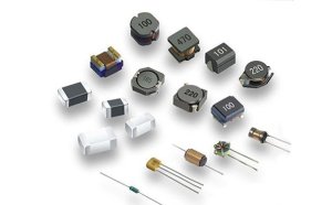
Embedded components are electrical parts that are placed inside the multilayer stack-up rather than soldered onto the outer surfaces. They take three main forms. Planar passives are created directly from copper geometry or resistive and capacitive materials laminated into an inner layer. Discrete thin components, such as 0201-size resistors and ceramic capacitors, are routed into cavities or placed on inner-layer copper before lamination. Finally, bare integrated-circuit dies can be attached to a core layer and connected through microvias, effectively hiding a silicon chip inside the board.
This is fundamentally different from conventional PCB assembly, where every component sits on the surface and is processed through solder paste printing, placement, and reflow. Once a part is embedded, it becomes part of the substrate itself: lamination encapsulates it, and only its electrical connections reach the outside world. That structural change is exactly what delivers the benefits — and the risks — discussed below.
Why Miniaturization Pressure Is Accelerating the Embedded Components Trend
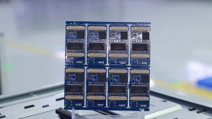
Component shrinking has real limits. Packages have moved from 0402 to 0201 and even 01005, yet placement yield, inspection capability, and solder-joint reliability all degrade as parts get smaller. Meanwhile, wearables, TWS earbuds, implantable medical electronics, and dense 5G modules keep asking for more function in less volume. When the outer surfaces of a board are already saturated, the only direction left is inward.
Embedding passives frees valuable surface real estate for connectors, RF front-ends, and shielding structures. It also shortens the electrical path between a die and its decoupling capacitors from several millimeters to a fraction of a millimeter, which matters enormously for high-speed and RF designs. Industry roadmaps from iNEMI and IPC have tracked embedded passives and embedded die for years, and production adoption is now visible in smartphone RF modules, automotive radar, and medical sensor boards — a clear signal that the trend has moved past the pilot stage.
How the Embedded Components Manufacturing Process Works
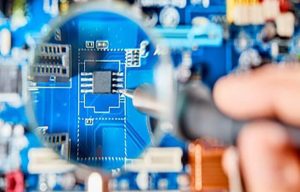
The process begins at the bare-board level, long before standard SMT assembly. For discrete embedding, a pick-and-place machine with die-attach accuracy places bare components onto inner-layer copper using epoxy or solder attach materials. The populated inner layers are then laminated under heat and pressure, burying the parts inside the stack-up. Laser or mechanical drilling creates microvias that reach the embedded terminals, and plating establishes the electrical connections.
Planar passives follow a different route. Resistive elements are printed or laminated from carbon- or thin-film resistive foils, while planar capacitors use high-permittivity ceramic-filled dielectric layers. Because these structures are formed by etching rather than placement, they eliminate individual component handling entirely. After lamination, the board enters conventional PCB assembly: outer-layer solder paste printing, component placement, reflow, and inspection proceed as usual. The embedded layers simply become invisible, highly protected infrastructure inside the finished board.
Electrical and Reliability Advantages of Embedding Passives in PCB Assembly
The electrical case for embedded components rests on interconnect physics. Every millimeter of trace between a processor die and its decoupling capacitor adds parasitic inductance that degrades power integrity at high frequencies. Placing the capacitor directly beneath or beside the die inside the stack-up can reduce that loop inductance by an order of magnitude, which is why embedded decoupling is popular in high-speed digital and RF modules.
Reliability improves as well. Laminated inside the board, components are shielded from moisture, flux residues, handling damage, and mechanical stress during secondary assembly. They cannot tombstone, skew, or suffer from solder-joint fatigue the way surface parts can, and they are invisible to the electrostatic discharge and contamination risks of the assembly line. For shock- and vibration-prone products such as automotive electronics and industrial sensors, this environmental protection is often a stronger argument than the space savings alone.
Cost and Supply-Chain Trade-Offs of Embedded Components
The economics are the hard part. Embedded parts cannot be reworked: a defective die discovered after lamination can scrap an entire multilayer panel, so yield must be managed layer by layer. Bare dies must be sourced as known-good die, often with different packaging, test documentation, and supply agreements than standard SMD parts. Engineering charges are higher because inner-layer artwork, cavity design, and lamination tolerance all demand careful co-design between the designer and the PCB assembly manufacturer.
On the other side of the ledger, embedding removes thousands of passive placements from the SMT line, reduces solder paste consumption, eliminates some inspection steps, and can shrink the board enough to cut substrate area. At high volumes, those savings can offset the added fabrication cost. The break-even point depends heavily on volume, layer count, and how much surface area is genuinely recovered, which is why a transparent cost model — not a rule of thumb — should drive the decision.

A Practical Selection Guide for Embedded Components in PCB Assembly
Embedded technology is a tool, not a default. The table below summarizes where it typically pays off and where conventional surface-mount remains the smarter choice.
| Application Scenario | Recommendation | Primary Reason |
|---|---|---|
| RF modules, decoupling-critical digital boards | Embed selectively | Parasitic reduction and signal integrity gains |
| Ultra-thin wearables and medical sensors | Embed aggressively | Surface real estate and thickness savings |
| High-shock automotive or industrial products | Embed sensitive parts | Environmental and mechanical protection |
| Low-volume prototypes and early builds | Keep SMD | NRE and scrap risk dominate at low volume |
| Cost-driven consumer boards with free space | Keep SMD | No area constraint to justify the premium |
| Designs needing frequent field rework | Keep SMD | Embedded parts are not serviceable |
A useful intermediate step is partial embedding: place only the highest-value passives or one critical die inside the board and keep everything else on the surface. Many production designs adopt this hybrid model first, then expand embedding coverage as yield data accumulates.
Design and DFM Rules for Successful Embedded Component Assembly
Successful embedding is decided at the design stage, long before any panel is laminated. The following checklist captures the practices that separate smooth programs from expensive ones.
- Source bare dies and thin passives only from suppliers who can certify known-good-die status with documented test data.
- Match the coefficient of thermal expansion between die attach, copper, and laminate to limit stress during reflow and thermal cycling.
- Define cavity tolerances and placement keep-outs jointly with the fabricator, since lamination squeeze-out can shift thin components.
- Build test coupons into the panel to verify embedded layer connectivity without destroying production boards.
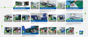
- Plan X-ray or acoustic inspection checkpoints after lamination to catch voids, cracks, and misalignment early.
- Maximize panel utilization, because every scrapped panel carries the full cost of all embedded parts inside it.
Design for testability deserves equal attention. Once components are buried, in-circuit test loses access to those nodes, so functional test coverage and boundary-scan strategy must be designed around the embedded regions rather than retrofitted afterward.
Embedded Components Compared With SiP and HDI Alternatives
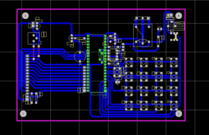
Embedded technology competes with two other miniaturization paths. System-in-Package integration moves multiple dies and passives into a molded module that is then placed as a single component — fast to adopt, but it adds a package layer and depends on module suppliers. HDI PCB assembly uses microvias, fine lines, and stacked via structures to pack more interconnect into less area without hiding any parts. Embedded components occupy a distinct middle ground: they keep the design in a single substrate, avoid module lead times, and preserve the flexibility that full SiP integration surrenders.
The three approaches are complementary rather than exclusive. A typical advanced design today might use an HDI stack-up, embed its decoupling capacitors and one power die, and mount a pre-integrated SiP module for the radio section. The right combination depends on volume, supplier ecosystem, and how aggressively the product roadmap demands thinness.

What to Expect From PCB Assembly Suppliers Offering Embedded Capability
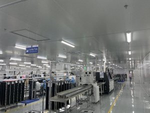
Not every PCB assembly manufacturer can execute embedding, so supplier selection deserves scrutiny. Ask for demonstrated die-attach placement accuracy, documented lamination process control, and microsection or X-ray evidence from prior embedded programs. A capable partner will also co-review your inner-layer artwork, propose coupon strategies, and model yield stacking honestly before committing to a price — the hallmarks of a genuine one-stop PCBA solution rather than a fabrication-only service.
Expect the conversation to start with a pilot: a small panel run with embedded coupons, followed by cross-sections and reliability testing before volume release. Suppliers with mature embedded capability will treat that pilot data as the foundation of a long-term yield agreement. If a partner quotes embedded work without asking for design files, die sourcing details, and reliability targets, treat it as a warning sign rather than a bargain.
Summary
Embedded components are moving from niche to mainstream because surface-mount miniaturization is hitting physical and economic limits. Embedding passives and bare dies inside the PCB substrate shortens critical electrical paths, protects sensitive parts, and reclaims surface real estate, at the cost of higher NRE, unrecoverable yield risk, and stricter design discipline. The best first step is selective embedding of high-value components, validated with coupons and inspection, and executed with a manufacturing partner who co-owns the yield model.
FAQ
Are embedded components reliable over the long term?
Yes, when die attach materials and CTE matching are engineered correctly. Laminated parts are protected from moisture, contamination, and mechanical shock, and field data from automotive radar and medical designs shows survival rates equal to or better than equivalent surface-mounted parts.
Can an existing SMD design be converted to embedded components?
Partially. Passives and one or two dies can usually be moved into inner layers with artwork changes, but a full conversion requires re-flooring the layout, updating test strategy, and re-qualifying the board, so hybrid conversion is the practical path for most products.
What production volume justifies embedded components?
Most programs become economical somewhere between tens of thousands and hundreds of thousands of units, depending on layer count, die cost, and how much surface area is recovered. Below that range, the NRE and scrap risk usually outweigh the savings.
Do embedded parts comply with industry qualification standards?
IPC and JEDEC have published guidelines covering embedded passive materials, die attachment, and cavities, and automotive customers routinely qualify embedded designs through AEC-Q based validation plans, so compliance is achievable with disciplined documentation.