

Every dollar spent on DFM review before production saves ten dollars in rework, delays, and scrap. Yet many design teams rush to fabrication without a thorough manufacturability assessment. This guide captures the key DFM principles. These principles separate smooth production launches from expensive firefights.
1.What Is DFM and Why Does It Matter?
Design for Manufacturability (DFM) is the practice of anticipating assembly constraints during the design phase. The cost of fixing a defect escalates exponentially as production progresses. This is illustrated in the table below.
| Phase | Relative Cost to Fix |
| Design phase (DFM catch) | 1x |
| Stencil fabrication | 3x |
| First-article assembly | 10x |
| Volume production | 50x+ |
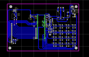
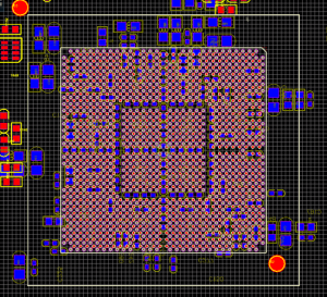
2.Component Selection and Spacing
Insufficient clearance is the most common DFM issue. Tight spacing creates solder bridging risks. It also limits inspection access, complicates rework, and reduces placement throughput. The following table outlines the minimum edge-to-edge spacing requirements for common component types.
| Component Type | Minimum Edge-to-Edge Spacing |
| 0201 passives | 0.3 mm |
| 0402 passives | 0.4 mm |
| 0603 passives | 0.5 mm |
| 0805 passives | 0.6 mm |
| QFP packages | 1.0 mm |
| BGA packages | 3.0 mm |
| Connectors | 2.0 mm from ICs |
3.Pad Design and Footprint Geometry
Pads must match component lead dimensions precisely. Oversized pads invite excessive solder volume and bridging. Undersized pads produce weak joints. The table below details pad design specifications for common package types.
| Package Type | Pad Width | Pad Length Extension |
| 0201 chip | 0.9–1.0x lead width | 0.15–0.25 mm |
| 0402 chip | 0.9–1.0x lead width | 0.2–0.3 mm |
| 0603 chip | 0.9–1.0x lead width | 0.25–0.35 mm |
| QFP (0.5mm+ pitch) | 1.0x lead width | 0.5–0.8 mm toe |
| QFN/DFN thermal pad | 0.8–0.9x pad size | 50–70% paste coverage |
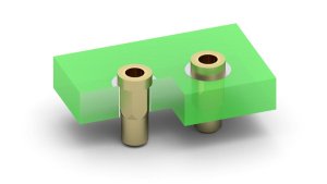
4.Fiducial Requirements
Place three global fiducials near board corners in an L-shaped arrangement. Use a minimum 1.0 mm diameter pad. Ensure 2.0 mm solder mask clearance around the pad. Local fiducials within 5 mm of fine-pitch components improve placement accuracy.
5.Test Point Design
| Parameter | Minimum | Recommended |
| Diameter | 0.8 mm | 1.0 mm |
| Spacing | 2.0 mm CTC | 2.5 mm |
| Clearance from component | 1.0 mm | 2.0 mm |
| Coverage | 60% of nets | 90%+ |
6.Stencil Design Considerations
The area ratio must exceed 0.66 for reliable paste release. For mixed component sizes, step-down stencils are ideal. They optimize paste volume across diverse requirements.
7.Panelization Guidelines
A rail width of 5–10 mm provides adequate handling margin. Maintain 2.0–3.0 mm board-to-board spacing. Place tooling holes with a 2.0–3.0 mm diameter. Keep components a minimum of 3.0 mm from panel edges.
Frequently Asked Questions
Q: How early should I engage a manufacturer for DFM? As soon as the preliminary layout is complete. Early feedback on component placement, spacing, and routing is valuable. It allows revisions without disrupting the design schedule.
Q: What files are needed for a DFM review?
Gerber RS-274X files, a complete BOM with manufacturer part numbers, a centroid file, and assembly drawings.
Q: Can DFM rules be relaxed for prototype builds? Some rules are absolute. Others are just guidelines. For prototypes with extremely tight density, teams like Keepbest evaluate case-by-case. They also flag any accepted risks explicitly.
Q: What is the most expensive DFM mistake you have seen? A medical device board had no test point coverage. It required full functional testing as the only verification. A single wrong resistor value passed at room temperature. But it failed in the field, resulting in a recall that exceeded $500,000.
Q: Is DFM review complimentary? For many manufacturers, including Keepbest, DFM feedback is complimentary. This applies to customers requesting production quotes.
Ready for a DFM review? Send your Gerbers, BOM, and centroid files to your engineering team. They will provide detailed feedback within 48 hours.