Schematic & PCB design
Circuit development, component placement and routing around your electrical and mechanical requirements.

KeepBest / PCB Design Services
Schematic design, PCB layout and product engineering support—with manufacturing in view from the start.
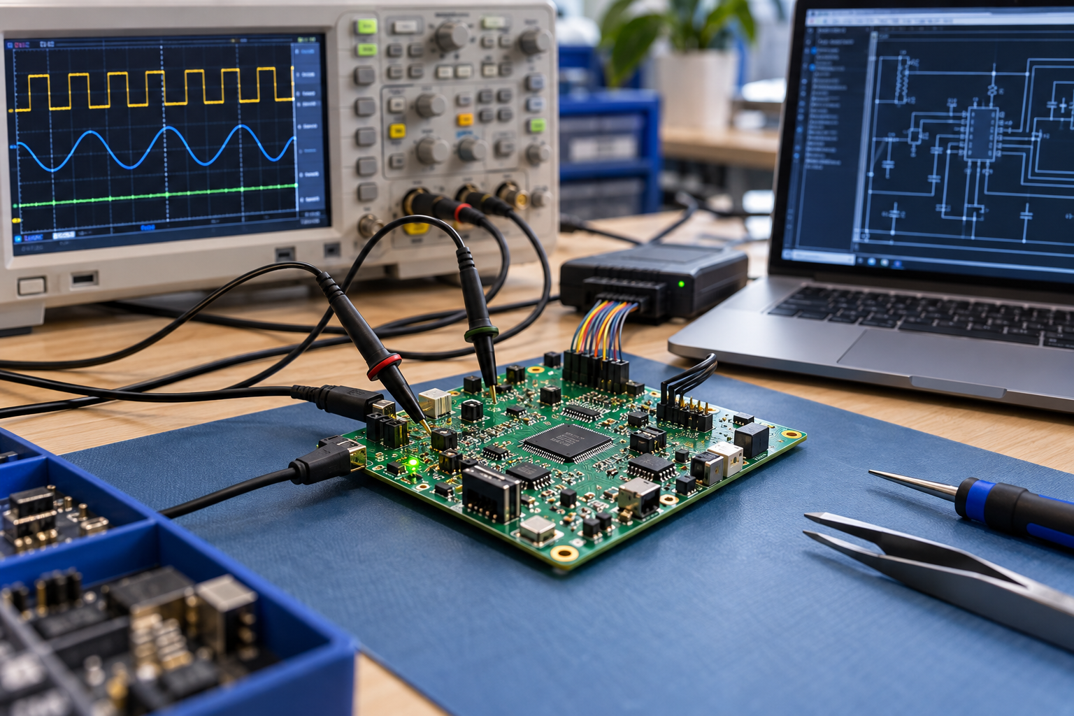
AI-generated design illustration · not a company photograph

Research & development support
KeepBest’s design services connect hardware, embedded engineering and manufacturing support. Work with us on a new design, an existing schematic or a board revision.
Circuit development, component placement and routing around your electrical and mechanical requirements.
Embedded and driver optimization, software/App development and algorithm support within the agreed project scope.
DFMA and 3D CAD support connect the design with fabrication, assembly and mechanical fit.
What we do
Bring the complete project or the part that needs engineering support. We agree the work and outputs around your requirements.
Translate product functions, interfaces and power requirements into the circuit design.
Placement, footprints, routing and board structure—including high-speed or high-density constraints specified for the project.
Discuss embedded/driver work, software/App development and algorithms as clearly defined engineering tasks.
Review fabrication, assembly and cost considerations, with 3D CAD output where agreed. Explore DFMA →
How we work
Scope, review points and delivery are agreed for each project.
Send your brief or current design, board constraints and target timing. We identify the work and missing inputs.
Progress the agreed schematic, layout or engineering tasks, with open questions and changes reviewed together.
Review the agreed outputs and revision before moving into PCB fabrication, assembly or further development.
Bring native schematic/PCB files where available, plus the BOM, board outline and relevant fabrication or assembly data. For high-speed or HDI work, include interface/data-rate constraints, stack-up, trace/spacing, via structure and BGA requirements. Timing depends on the inputs and actual complexity.
Confirm the CAD tool/version and required outputs: editable design files, BOM, Gerber/drill data and 3D CAD as applicable. Related 3D or CNC work can be discussed separately.
Yes. Share the intended functions and constraints, or your existing schematic/layout and the changes you need. We confirm the inputs and engineering scope before work begins.
Altium Designer, Cadence OrCAD/Allegro, Eagle and KiCad are included in our service information. Share your software version so file compatibility and handoff formats can be confirmed.
Embedded, driver, software/App and algorithm support are available to discuss. They are quoted as agreed scope, rather than automatically included in every PCB layout project.
Input completeness, design complexity, constraints, required outputs and review cycles. Send your target date with the current files so the proposal can set out the schedule assumptions.
Talk to KeepBest
Send your requirements or current files. Tell us what you need to develop, review or improve.
Prefer email?
sales@keepbestpcba.com ↗
Fields marked * are required. Phone is optional.
Enquiries follow our Privacy Policy.