
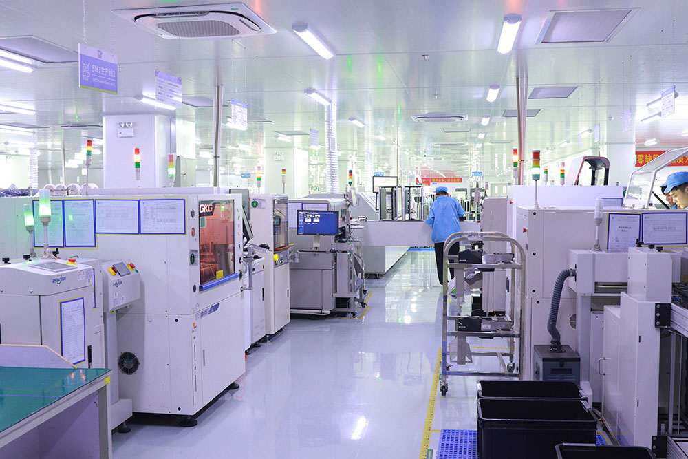
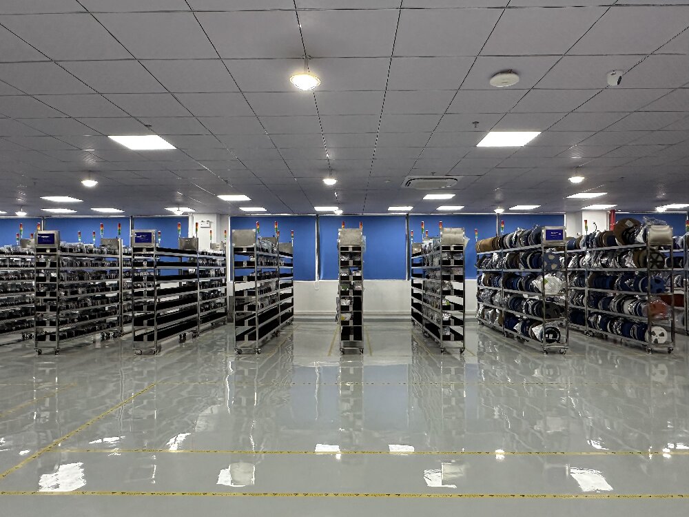
Ultra-miniature passives have moved from laboratory curiosity to volume production reality. The 01005 case size measures just 0.4 mm by 0.2 mm, roughly the footprint of a grain of salt, and it now appears on smartwatch mainboards, hearing-aid modules and dense RF front ends. Yet very few lines can place and solder it at an acceptable yield. Reliable 01005 component assembly is less about buying a newer placer and more about controlling every variable upstream: paste volume, placement force, reflow soak and inspection resolution. This article follows a real wearable sensor project through each of those stages and shows which parameters actually moved first-pass yield.
01005 Components Push SMT Assembly Beyond Conventional Process Limits
A 01005 chip resistor has a mass of roughly 0.04 mg. Its termination width is about 0.1 mm, and the recommended pad is typically 0.18 mm by 0.09 mm with a 0.09 mm gap. At that scale, the surface tension of the molten solder becomes comparable to the weight of the part, so any imbalance in paste volume or heat distribution pulls the component upright instead of letting it settle.
The physical constraints cascade. A stencil thick enough to release paste for an 0402 body is too thick for a 01005 aperture, because the area ratio falls below the practical release limit. Placement tolerance that is comfortable at 0603 becomes marginal, and a vision system calibrated for larger bodies struggles to distinguish a 01005 termination from a dust particle. None can be solved in isolation.
There is also a metrology problem. If the paste deposit is 0.09 mm wide and the camera samples at 20 micrometres per pixel, the measured volume carries more noise than the process signal, and operators tune against measurement error.
A Wearable Sensor Case Study Defined the 01005 Assembly Challenge
The project was a six-layer HDI rigid-flex board, 0.6 mm thick, for a wrist-worn biosensor. The panel carried 412 placements, of which 96 were 01005 decoupling capacitors and resistors concentrated around a power management IC. The customer required IPC-A-610 Class 3 and first-pass yield above 95 percent.
The first production lot returned 71 percent first-pass yield. Defect pareto showed three dominant modes: tombstoning at 41 percent of defects, insufficient solder at 27 percent, and missing components at 18 percent. Notably, no bridged joints appeared, which pointed away from over-printing and toward release and placement instability.
Cross-sections confirmed the diagnosis. Paste deposits on the 01005 pads averaged 62 percent of nominal volume with high variance, and several joints showed the component standing on one termination. The team rebuilt the process window in four stages rather than adjusting single machine settings.
Solder Paste Printing Controls Decide 01005 Assembly Yield
Printing accounts for the majority of 01005 defects, and the case study confirmed it. The original stencil was 0.12 mm laser-cut stainless steel without coating. Reducing thickness to 0.08 mm raised the area ratio from 0.44 to 0.66, which sits inside the reliable release window for a 0.18 mm by 0.09 mm aperture.
Paste selection mattered just as much. Type 4 powder with 20 to 38 micrometre spheres cannot pass a 90 micrometre aperture consistently, so the line switched to Type 5 paste in the 15 to 25 micrometre range. The finer powder costs more and has a shorter floor life, which is why many factories resist the change.
Machine parameters were then narrowed deliberately. Squeegee pressure dropped to 4.5 kg with a 60 degree metal blade, print speed fell to 20 mm per second, and a nano-coating was applied to the aperture walls to reduce adhesion. Post-print inspection moved to a 2 micrometre resolution 3D system measuring volume, area and height at every 01005 pad rather than sampling.
- Stencil thickness: 0.08 mm, laser-cut, nano-coated
- Area ratio target: above 0.66 for every 01005 aperture
- Paste type: Type 5, 15 to 25 micrometre powder, lead-free SAC305
- Print speed: 20 mm/s with 60 degree squeegee at 4.5 kg
- Separation speed: below 3 mm/s to avoid paste scooping
- SPI sampling: 100 percent on 01005 pads during ramp-up
After these changes, average deposit volume rose to 94 percent of nominal with a standard deviation cut by more than half, and tombstoning dropped sharply in the next lot.
Placement Accuracy and Nozzle Selection Drive 01005 Component Assembly
Placement is where machine specifications meet reality. The equipment was rated at 35 micrometres at three sigma, but that figure assumes a clean nozzle, a stable feeder and a centred component, and each assumption needed attention.
The nozzle was changed from a 0.3 mm to a 0.18 mm ceramic tip with a compliant rubber core, and pickup force was reduced to 0.3 newtons. Excessive force tilts the part, which the vision system then centres incorrectly. A dedicated 01005 vision library with backlighting and a smaller field of view eliminated the dust false-rejects that had been stopping the line.
Feeder performance proved equally important. Tape peel force above 0.1 newtons vibrates the pocket and can flip a 01005 part before the nozzle arrives. The team specified deep-pocket embossed tape, replaced worn peel bars, and cut placement speed on 01005 feeders by roughly 35 percent. Cycle time rose four seconds per board, a trade the yield curve repaid.
Reflow Profiling for 01005 Assembly Balances Tombstoning and Voiding
Small thermal mass changes everything about reflow. A 01005 body heats and cools far faster than the surrounding laminate, so a profile that is gentle for a 15 mm power module can still shock the miniature passives. The profile was rebuilt around measured thermocouples attached directly beside the 01005 cluster.
Ramp rate was held between 1.5 and 2.0 degrees Celsius per second, soak ran from 150 to 180 degrees Celsius for 60 to 90 seconds, and peak temperature was set at 237 degrees Celsius with 55 seconds above liquidus. Nitrogen was introduced at below 1,000 ppm oxygen, which improved wetting on the small pads and reduced the oxide-driven imbalance that causes tombstoning.
The team also verified that both terminations reached liquidus within two seconds of each other. Where a ground plane pulled heat away asymmetrically, thermal relief spokes were added in the next board revision, which is often the only permanent cure for a stubborn tombstoning rate.
Inspection of 01005 Joints Requires Higher-Resolution AOI and X-ray
Inspection at this scale is a capability question, not a preference. The existing AOI ran at 20 micrometres per pixel, adequate for 0402 but unable to resolve a fillet on a 0.1 mm termination. Upgrading to a 10 micrometre optical system with side-view lighting made the fillet visible without increasing false calls, because the extra resolution reduced ambiguity rather than adding noise.
X-ray was reserved for bottom-terminated packages and for voiding under thermal pads, since 01005 joints are thin enough that transmission imaging adds little. Functional test replaced in-circuit test, because probe access on a 0.6 mm HDI board was not available at that density.
The most useful inspection change was statistical rather than optical. Logging defect location by panel position revealed two feeders drifting after several hours of production, a pattern invisible in aggregate yield numbers.
Standard and 01005 Assembly Process Parameters Compared
The table below summarizes the parameter shift between a conventional 0402-capable line and the 01005-capable configuration used in the case study. It is a practical starting point, not a universal recipe, because board thickness, copper balance and paste chemistry all shift the window.
| Parameter | Standard 0402 line | 01005-capable line |
|---|---|---|
| Stencil thickness | 0.12 mm | 0.08 mm |
| Aperture area ratio | 0.60 to 0.70 | above 0.66, nano-coated |
| Solder paste type | Type 4, 20 to 38 micrometre | Type 5, 15 to 25 micrometre |
| Placement accuracy | 60 micrometre at 3 sigma | 35 micrometre at 3 sigma |
| Nozzle tip | 0.3 mm rubber | 0.18 mm ceramic with rubber core |
| Pick force | 1.0 N | 0.3 to 0.5 N |
| Placement speed on small parts | 100 percent | 60 to 65 percent |
| Reflow ramp | 2.5 degrees C per second | 1.5 to 2.0 degrees C per second |
| Atmosphere | Air | Nitrogen below 1,000 ppm O2 |
| AOI resolution | 20 micrometre per pixel | 10 micrometre per pixel |
Handling, Packaging, and ESD Control Protect 01005 Components
A 01005 part that leaves its pocket is effectively lost, and the counting problem is real. Standard reel reconciliation assumes a few percent of attrition, but with 01005 small losses compound into line stops. The project adopted embossed tape with 8 mm width and deep pockets, verified peel force on incoming reels, and reconciled reel counts at every shift change.
Handling discipline extended to rework. Technicians used vacuum wands rather than tweezers, worked over a tacky mat to catch dropped parts, and kept an anti-static workstation with ionized air. Moisture control followed MSL rules, with bake schedules based on package-level data rather than board thickness.
This is where experience separates a capable PCB assembly manufacturer from one that simply owns a modern placer. The equipment list is identical in both cases; the difference sits in how tightly the upstream variables are held.
ESD protection needed review as well. Smaller bodies tolerate less energy before damage, and peeling cover tape generates significant charge. Grounded peel bars, humidity above 30 percent RH and continuous wrist-strap verification kept field failures from appearing months later as leakage.
Cost and Yield Economics of 01005 Assembly in Volume Production
01005 adoption is almost always driven by board area. Replacing 0402 decoupling with 01005 freed roughly 30 percent of the area around the power management IC in the case study, which allowed a smaller rigid-flex outline and a lighter device. That mechanical benefit, not component cost, is the business case.
The cost side is less obvious. Type 5 paste costs more and expires faster, throughput drops by a third on those feeders, and AOI programming hours increase. Yet the defect cost per occurrence is high, because a tombstoned 01005 is invisible to the naked eye and becomes a field return rather than line scrap.
In the case study, first-pass yield climbed from 71 to 93.6 percent across three lots, reaching 96.1 percent after the thermal relief revision. Scrap value was negligible; the savings came from eliminating rework hours and from avoiding a second inspection station that had been planned as a workaround.
A team that already controls stencil design, paste management and inspection under one roof, which is the practical definition of a one-stop PCBA solution, can absorb that learning curve before the first production lot instead of discovering it lot by lot.
Summary
01005 component assembly is a system problem. Paste deposit, placement force, reflow profile and inspection resolution share one narrow window, and improving a single element produces little yield gain. The case study moved from 71 to 96 percent first-pass yield by rebuilding the window in sequence: stencil and paste, then placement, then reflow, then inspection. Printing comes first because it is the largest contributor and the cheapest to correct.
FAQ
Can a standard SMT line run 01005 components without new equipment?
Often yes, but not without changes. A modern placer with a 01005 vision library, a thinner nano-coated stencil, Type 5 paste and a higher-resolution AOI will handle most designs. The limiting item is usually inspection rather than placement.
Why do 01005 parts tombstone more than 0402 parts?
The mass is so low that surface tension dominates. Any imbalance in paste volume, pad geometry or heat reaching the two terminations will lift one end. Symmetric apertures and thermal reliefs on ground planes remove most of the root cause.
Is nitrogen reflow mandatory for 01005 assembly?
It is not mandatory, but it widens the process window noticeably. Lower oxygen improves wetting on small pads and reduces the oxide imbalance that drives tombstoning, which matters most during ramp-up and on boards with mixed finishes.
Keywords
01005 component assembly, ultra-miniature SMT assembly, 01005 placement accuracy, Type 5 solder paste, fine-pitch stencil printing, tombstoning control, HDI PCB assembly, SMT process capability, AOI inspection resolution, micro component handling
Tags
01005 component assembly, ultra-miniature SMT assembly, micro component placement, fine-pitch stencil printing, SMT process control, tombstoning defects, HDI PCB assembly, PCB assembly manufacturer