
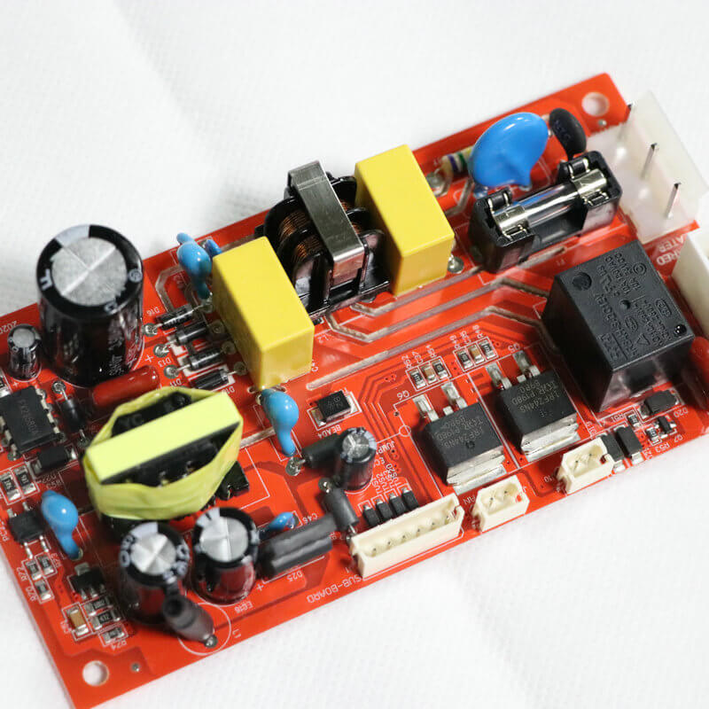

Every PCB design team has lived through the same nightmare: a beautifully laid-out board that the factory rejects during new product introduction. The root cause is almost never the design itself — it is the gap between what works in EDA software and what works on a pick-and-place line. A thorough DFM analysis (Design for Manufacturability analysis) closes this gap before prototypes leave the lab, saving thousands of dollars in re-spins and weeks of schedule slip.
DFM analysis is the systematic review of a PCB design against the physical realities of SMT PCB assembly and through-hole manufacturing. It examines every aspect of the board — component spacing, pad geometry, thermal relief, solder mask clearances, and test point placement — through the lens of factory floor constraints. When performed early and iteratively, it transforms a good design into a production-ready product that assembles with high first-pass yield and predictable cost.
What Is DFM Analysis and Why Does It Matter
DFM analysis is the bridge between PCB design engineering and electronics manufacturing. It ensures that every footprint, every clearance, and every layer stack decision translates correctly into the automated equipment running on a modern assembly line. Without it, even boards that pass electrical DRC can fail catastrophically during reflow soldering, wave soldering, or automated optical inspection.
The financial stakes are substantial. Industry data consistently shows that design issues caught during DFM review cost roughly 10 times less to fix than issues caught during prototyping, and 100 times less than those discovered in production. For a typical mid-volume run, a single board re-spin triggered by an overlooked DFM violation can cost $15,000 to $40,000 in engineering time, tooling charges, and delayed revenue.
Key Objectives of DFM Analysis
- First-pass yield improvement: Detecting and correcting layout issues that cause tombstoning, bridging, opens, or insufficient solder joints before the first board is built.
- Assembly cost reduction: Ensuring the design is compatible with standard panel sizes, standard component packaging, and automated equipment capabilities — reducing manual intervention and rework.
- Supply chain alignment: Verifying that every BOM component is available in production quantities, from approved sources, and in packaging formats supported by the assembly line feeders.
- Test coverage assurance: Confirming that ICT and flying probe test points are physically accessible and that boundary-scan chains are correctly implemented.
Step 1 — Component Selection That Considers Manufacturing Reality
The DFM analysis process starts before a single trace is routed. Component selection is the single most influential design decision affecting downstream manufacturability. A perfectly designed footprint for a component available only on 24-week lead time, or in a package incompatible with the assembly line’s feeder configuration, creates an instant manufacturing bottleneck.
PCB components procurement should be treated as a design constraint, not an afterthought. During the component selection phase, verify the following for every BOM line item:
- Package availability: Does the chosen component have an alternate source? Single-sourced components with volatile lead times are the single largest cause of production delays in PCBA manufacturing.
- Packaging format: Is the component available in tape-and-reel? Components supplied in tubes or trays require different feeder hardware and can slow down automated SMT placement.
- MSL rating: Moisture Sensitivity Level dictates storage, baking, and floor-life requirements. Level 3 and higher components demand controlled handling environments that add cost and complexity.
- Minimum order quantity alignment: Prototyping runs using components with 5,000-piece MOQs waste capital and shelf space. Match component selection to production volume expectations.
Working with an experienced PCB assembly manufacturer during the component selection phase adds immediate value. Their procurement teams track real-time market conditions — allocations, end-of-life notices, and price volatility — across hundreds of distributor and manufacturer channels, information that EDA libraries do not surface.
Step 2 — Footprint and Land Pattern Verification
Footprint accuracy is where DFM analysis delivers its most concentrated return on effort. A single incorrect pad dimension on a QFN or BGA package can produce open circuits, head-in-pillow defects, or intermittent failures that pass electrical test but fail in the field.
The IPC-7351 standard defines three footprint density levels, and choosing the wrong one for your application is a common and costly mistake. Level A (Maximum) provides the largest lands for high-reliability applications such as medical or aerospace. Level B (Nominal) is suitable for most commercial and industrial products. Level C (Minimum) is for high-density consumer products where board real estate is at a premium — but it reduces process window and increases defect risk.
Critical Footprint Checks
- QFN thermal pad: The center pad must be segmented or have proper via pattern to prevent voiding. Voids exceeding 25% of the pad area degrade thermal performance and can cause field failures in power-management ICs.
- BGA ball-to-pad ratio: Pad diameter should be 80-85% of ball diameter. Oversized pads increase bridging risk; undersized pads reduce self-alignment during reflow.
- Chip component pad geometry: For 0402 and smaller passives, pad width should be equal to component width, and pad extension beyond the termination should be 0.15mm minimum. This balance prevents tombstoning while maintaining adequate solder fillet formation.
- Through-hole annular rings: Minimum 0.25mm annular ring for PTH components to ensure reliable solder wetting on both sides of the board.
Step 3 — Panelization and Board Edge Clearance
Individual PCBs do not run through assembly lines — panels do. The panelization strategy determines how many boards fit per panel, how they separate after assembly, and whether the assembly process can run at full automation speed. A poorly designed panel increases handling costs for every single board produced.
Effective panelization starts with understanding the assembly line’s conveyor width, which is typically 50mm to 350mm for standard SMT lines. The panel must include adequate rail clearance — typically 5mm on each edge — plus fiducial marks for automated optical alignment. Fiducials should be placed near three corners of the panel, at least 5mm from edges, and should be 1mm diameter pads with 2-3mm solder mask clearance.
Depaneling method is another decision that affects both design and cost. V-scoring is the most economical option for rectangular boards but limits component placement near board edges. Tab-routing with mouse bites is better for irregular shapes but adds routing cost and leaves rough edges that may require sanding. The depaneling method must be selected before layout so that keep-out zones are correctly defined around score lines and breakout tabs.
Step 4 — Thermal Management in PCB Layout
Thermal design directly impacts soldering quality. During reflow, every copper plane, via, and trace acts as a heat conductor — and this behavior must be accounted for in the DFM analysis.
The most common thermal DFM issue is cold solder joints on components connected to large copper planes. A small passive component with one pad connected to a solid ground plane will heat unevenly during reflow. The pad on the plane side remains cooler and may not reach proper wetting temperature before the flux activates and then burns off on the hotter side. The result is a one-sided solder joint — mechanically weak, electrically unreliable, and difficult to detect with visual inspection alone.
Thermal relief spokes are the standard solution. A thermal relief pad connects to the plane through narrow spokes — typically 0.25mm to 0.35mm wide — that restrict heat flow into the plane, allowing both pads to heat at similar rates. However, thermal reliefs reduce current-carrying capacity, so they must be sized appropriately for power paths and verified during electrical review.
Step 5 — Test Point Placement and Accessibility
In-circuit testing and flying probe testing require physical access to every net on the board. A design may pass every other DFM check but still fail during production if test points are buried under tall components, placed too close to board edges, or omitted entirely on critical nets.
ICT fixture-based testing typically requires test points on one side of the board, with a minimum pitch of 2.54mm (100 mil). Flying probe testing is more flexible — it can access both sides and tighter pitches — but is slower and more expensive per board for high-volume production. The choice between ICT and flying probe should be made during PCB prototyping assembly so that test point strategy aligns with the intended production test methodology.
- Place test points at least 2.5mm from component bodies to ensure probe clearance.
- Keep test points at least 5mm from board edges to avoid fixture interference.
- Distribute test points evenly to balance fixture pressure and avoid board flex during test.
- Include at least one test point per net; for critical nets, include two for redundancy.
Step 6 — Solder Mask and Silkscreen Optimization
Solder mask defines where solder can and cannot flow, and silkscreen provides the human-readable reference information that operators use during assembly, inspection, and rework. Both layers are easy to overlook during DFM analysis — and both can cause real manufacturing problems when done wrong.
Solder mask registration tolerance is typically 0.075mm for modern LDI (laser direct imaging) processes. This means that solder mask dams — the narrow strips of mask between adjacent pads — must be at least 0.1mm wide to be reliably produced. If the gap between pads is smaller than the minimum dam width, the mask opening should be combined into a single window covering both pads (a gang mask), accepting that solder bridging risk increases and must be managed through stencil design.
Silkscreen legibility degrades when text overlaps pads, vias, or board edges. The minimum line width for readable silkscreen is 0.15mm, and text height should be at least 1.0mm. Reference designators should be placed near — but not on — component bodies so they remain visible after assembly. For dense boards, consider moving reference designators to an assembly drawing rather than crowding the silkscreen layer.
Step 7 — Manufacturing File Review and Validation
The final DFM analysis step is a systematic review of the manufacturing output files before they are released to the factory. These files — Gerber data, drill files, BOM, pick-and-place (centroid) data, and assembly drawings — constitute the complete manufacturing package. An error in any one of them can stop production.
File-by-File DFM Checklist
- Gerber files: Verify that all layers are present and correctly named. Check that the board outline layer matches the mechanical dimensions and includes panelization features. Confirm that solder paste layers exist for all SMT pads and are correctly sized — paste aperture reduction for fine-pitch components should typically be 10-15% smaller than the pad.
- Drill file: Verify drill count matches the number of plated and non-plated holes in the design. Check that via sizes are within the manufacturer’s capability (typically 0.2mm minimum for mechanical drilling, 0.1mm for laser).
- BOM: Every reference designator must map to exactly one manufacturer part number and one internal part number. Manufacturer part numbers must be verified against current availability — a BOM that references an obsolete part number will cause immediate procurement delays.
- Pick-and-place file: Verify that all SMT components have centroid coordinates, rotation values match the manufacturer’s tape orientation, and the file format (usually CSV with units in millimeters) is correct. Missing or incorrect rotation is the most common pick-and-place error and causes entire reels of components to be placed with wrong orientation.
Many teams find that partnering with a one-stop PCBA solution provider simplifies this final review stage, because the manufacturer’s engineering team runs the same DFM checks natively within their CAM software before committing to production.
Common DFM Pitfalls That Delay Production
Even experienced design teams encounter recurring DFM issues that consistently delay NPI schedules and increase costs. Being aware of these common pitfalls helps teams catch them before they become production problems.
- Acid traps: Acute angles in copper traces (less than 90 degrees) can trap etchant chemicals during PCB fabrication and cause long-term corrosion. All trace angles should be 135 degrees or greater, and tee-junctions should use rounded or chamfered transitions.
- Copper thieving imbalance: Large empty areas on outer layers can cause uneven copper plating during fabrication. Copper thieving — adding non-functional copper patterns in empty areas — balances current density and ensures uniform plating thickness across the panel.
- Via-in-pad without filling: Placing vias inside SMT pads without capping or filling them causes solder to wick down into the via during reflow, starving the joint. Via-in-pad designs require filled and capped vias, which add fabrication cost.
- Insufficient component spacing: Components placed too close together prevent automated optical inspection cameras from getting clear views of solder joints and make rework nearly impossible. The IPC-A-610 standard provides minimum spacing guidelines by component height.
- Mixed technology without process sequencing: When a board includes both surface-mount and through-hole components, the assembly process sequence must be defined during DFM review. SMT components are placed and reflowed first, then through-hole components are inserted and wave-soldered — unless selective soldering is used.
Integrating DFM Analysis into Your Development Workflow
DFM analysis should not be a one-time gate review conducted days before Gerber release. It is most effective when integrated continuously into the development cycle, starting at the schematic stage and continuing through layout, prototyping, and production ramp.
Modern EDA tools embed basic DFM rule checks that catch gross violations during layout. However, automated checks cannot replace a manufacturer’s DFM engineering review, which applies process-specific knowledge — such as the exact conveyor width, preferred panel size, and specific feeder configurations available on the line that will build your boards.
The most efficient workflow is to submit the design for a preliminary DFM review at 70% layout completion, when enough geometry is in place for meaningful analysis but changes are still inexpensive. Address the flagged issues, complete the layout, and then submit a final DFM review before Gerber release. This two-stage approach catches systemic layout issues early while leaving room for final polish.
For teams engaged in PCB prototyping assembly, the DFM feedback loop is especially valuable because lessons learned during prototype assembly feed directly back into the next design iteration. Prototypes built without DFM review often exhibit different behaviors than production boards built on different equipment — making the prototype less useful as a validation tool.
Every hour invested in DFM analysis returns multiple hours of avoided rework, reduced troubleshooting, and faster time-to-market. The discipline of designing for manufacturability is not a constraint on creativity — it is the practice that turns creative designs into reliable products.
