
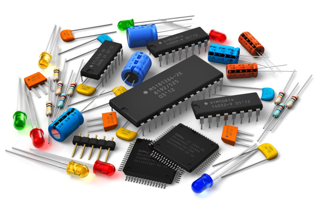
In the era of explosive growth of smart hardware—from wearable smartwatches to automotive domain controllers, from aerospace radiation-resistant modules to medical monitoring systems—the Printed Circuit Board Assembly (PCBA) has emerged as the “lifeblood” of electronic devices. Unlike PCB manufacturing, which provides the foundational circuit substrate, PCBA engineering represents the fusion of microelectronics and precision engineering, where surface-mount components (SMCs) and through-hole parts coexist in a microcosm of advanced manufacturing.
This process involves over 200 interdependent steps, spanning from 01005-sized component placement to 0.4mm-pitch BGA soldering, and from nanometer-level solder paste deposition to millisecond-precision reflow profile optimization. In cutting-edge fields like 5G communications, AIoT, and electric vehicles, PCBA technology has pushed boundaries with innovations such as 0.2mm-thin flex-rigid boards, laser direct imaging (LDI), and multi-layer blind vias, enabling circuit stacking exceeding 100 layers within sub-millimeter dimensions.
Design For Manufacturability (DFM) Analysis: The Foundation of Success
- Component compatibility: Ensuring footprints match standard dimensions (e.g., verifying 0402 resistors fit within solder pad tolerances).
- Thermal management: Flagging areas prone to heat buildup (e.g., high-power ICs adjacent to heat-sensitive capacitors).
- Assembly feasibility: Checking for tight clearances that could hinder pick-and-place accuracy or solder flow.
Lorem ipsum dolor sit amet, consectetur adipiscing elit. Ut elit tellus, luctus nec ullamcorper mattis, pulvinar dapibus leo.
Component Sourcing: Quality from the Start
- Authenticity: All components are traceable to original manufacturers, eliminating counterfeit risks.
- Rigorous IQC: Incoming parts undergo multi-stage inspections, including:
- Visual checks for physical damage (e.g., bent leads on connectors).
- Electrical testing (e.g., verifying capacitor values with LCR meters).
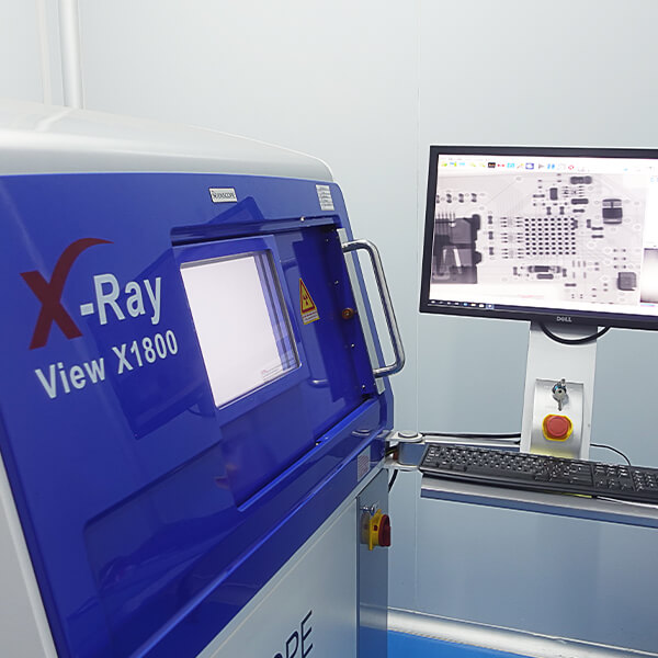
- X-ray scans for ICs to detect internal defects like die cracks.
PCB Fabrication: Precision in Every Layer
- Material selection: FR-4 for general applications, Rogers 4350B for high-frequency (5G) boards, and PI films for flexible PCBs in wearables.
- Advanced fabrication steps:
- Laser drilling: Achieving microvias (≤0.1mm) for high-density interconnects (HDIs).
- Sequential lamination: Enabling complex layer stacking for 12+ layer boards.
- Surface finish options: ENIG (Electroless Nickel Immersion Gold) for corrosion resistance or OSP (Organic Solderability Preservative) for cost-sensitive projects.
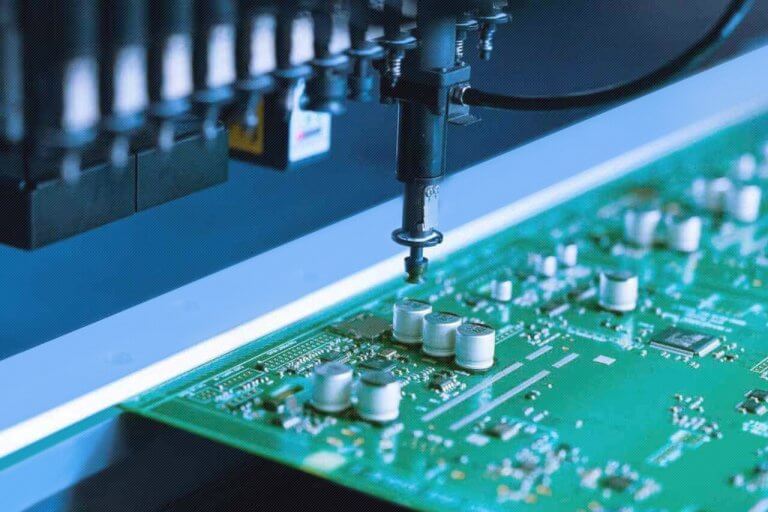
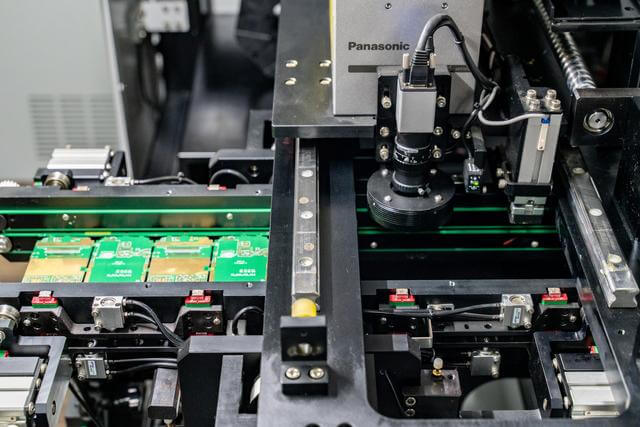
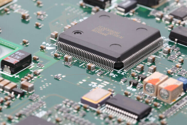
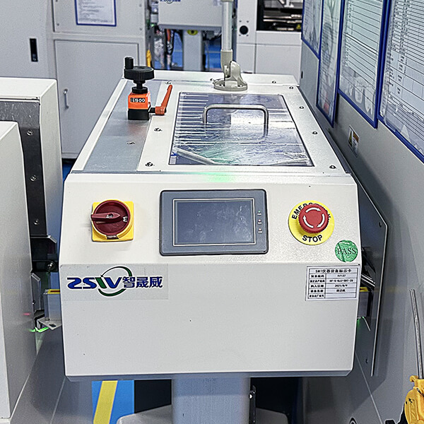
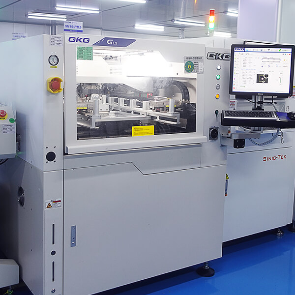
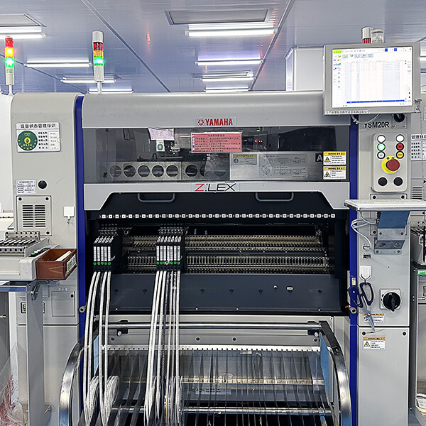
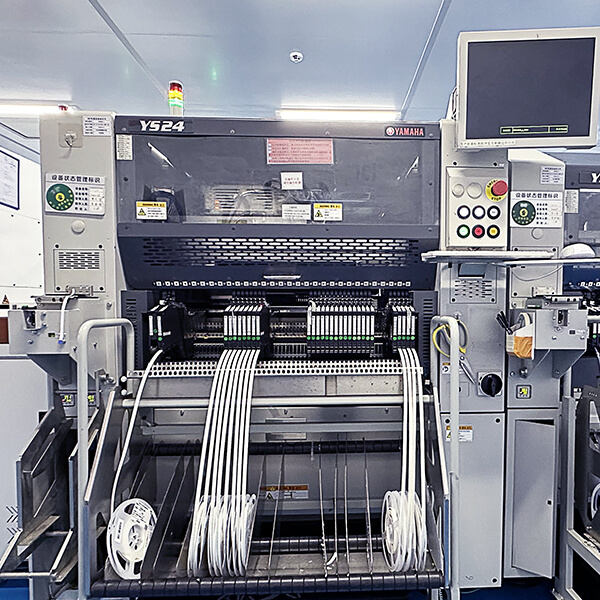
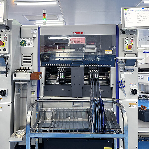
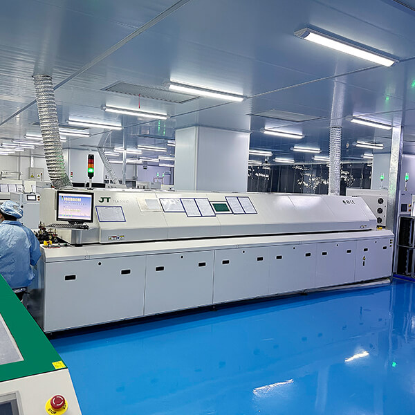
Surface Mount Technology (SMT) Assembly
- Solder paste printing: A stencil (laser-cut from 0.12mm stainless steel) deposits solder paste onto pads. A 3D SPI (Solder Paste Inspection) system immediately verifies volume (±5% tolerance) and uniformity, preventing defects like insufficient solder or bridging.
- Component placement: High-speed nozzles pick components from tape-and-reel or trays, guided by dual-camera vision systems that correct for component rotation or skew.
- Reflow soldering: PCBs pass through a nitrogen-enriched reflow oven with 10 temperature zones. The profile is tailored to solder paste specifications—e.g., lead-free alloys (SAC305) require peak temperatures of 245°C, while leaded variants (Sn63/Pb37) peak at 220°C. Nitrogen reduces oxidation, ensuring shiny, void-free solder joints.
Through-Hole & Mixed-Technology Assembly
- Automated insertion: Machines place through-hole parts with precision, reducing human error in high-volume runs.
- Wave soldering: A turbulent solder wave (250–260°C) wets component leads, with conveyor speed adjusted to ensure 3–5 seconds of contact time—critical for forming strong fillets.
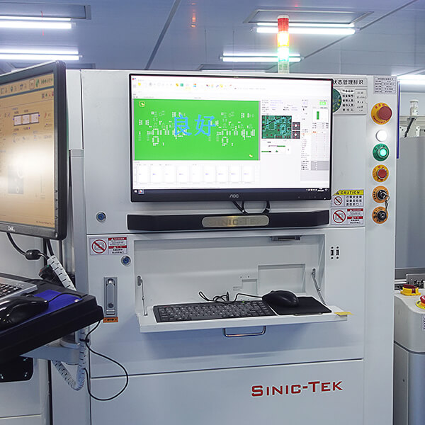
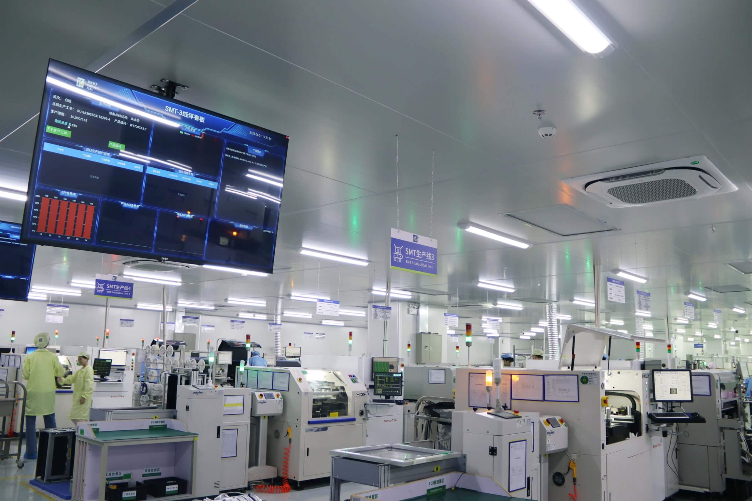
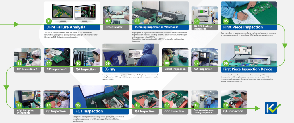
Comprehensive 19-step Inspection Process
- In-line checks: Operators use 10x magnification to inspect solder paste coverage and component alignment post-placement.
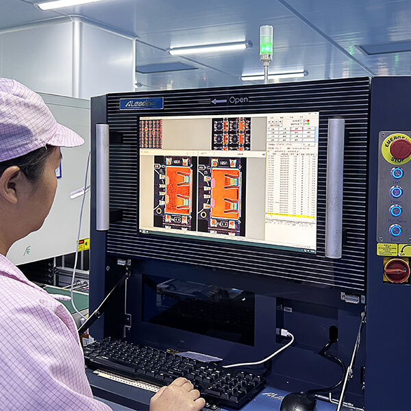
- 3D AOI: Cameras capture 2D and 3D images to detect defects like tombstoning (component lifting) or solder voids >15% of joint area.
- X-ray inspection: For BGA, CSP, and QFN packages, X-ray systems reveal hidden issues—e.g., bridging under BGA balls or incomplete wetting.
- Functional testing: Custom test fixtures validate electrical performance, from continuity checks to full system operation (e.g., verifying sensor output in IoT modules).
Box Build Assembly: From PCB to Product
- Mechanical integration (mounting PCBs in enclosures, securing cables with strain reliefs).
- Final testing (e.g., power-up checks, software loading, and calibration).
- Packaging (ESD-safe bags for sensitive electronics, custom cartons for shipping).
Conclusion
KeepBestPCBA’s assembly process is a testament to how technology and expertise converge to deliver excellence. By prioritizing DFM, rigorous sourcing, and advanced testing, they ensure each PCBA meets the demands of applications ranging from automotive control systems to industrial IoT sensors. For partners seeking reliability, scalability, and innovation, KeepBestPCBA’s process isn’t just a workflow—it’s a promise of quality.