
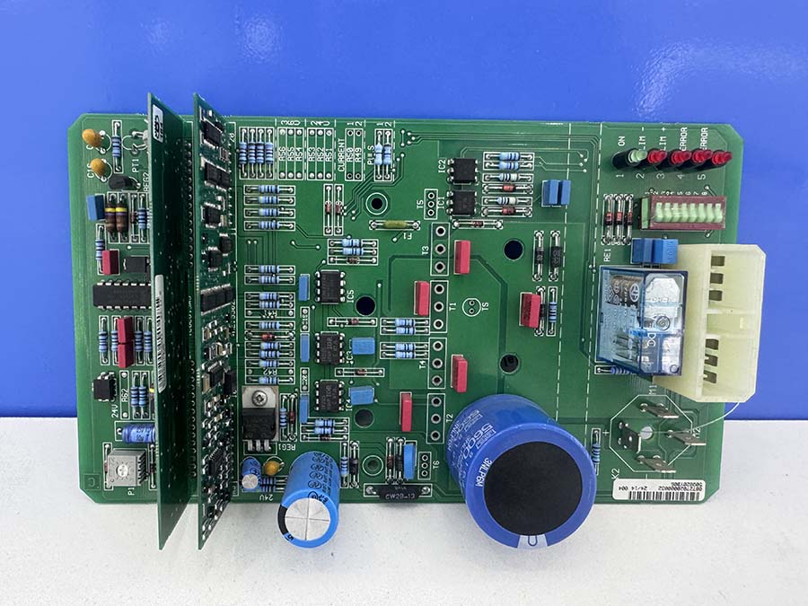
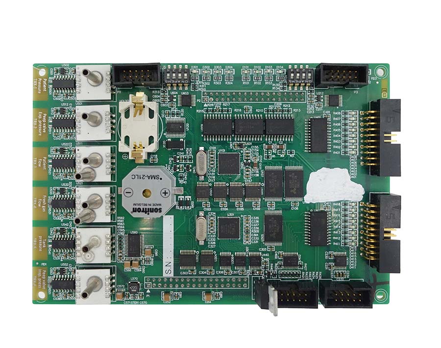
PCBA layout serves as the core component of electronic product design, directly impacting performance, cost, and reliability. This article systematically analyzes fundamental layout principles, key component rules, routing techniques, and thermal management strategies, providing electronics engineers with actionable, practical guidance.
1.Fundamental Layout Principles
1.1 Priority Strategy: Large First, Small Later; Difficult First, Easy Later
Layout implementation should follow spatial priority principles. Begin with large, heavy, and difficult-to-install components—typically large IC chips, heat sinks, transformers, and other structural elements. These components occupy significant space and have strict mounting requirements; prioritizing their placement prevents subsequent spatial conflicts. Subsequently, arrange small, easy-to-install resistors, capacitors, and inductors to maximize utilization of remaining space. This strategy effectively avoids rework or operational inconveniences caused by insufficient space later in the process.
1.2 Signal Flow Orientation
Layout planning must strictly follow schematic signal flow direction. Arrange signal sources, processing units, and terminal loads in logical sequence to ensure the shortest and smoothest signal transmission paths. This approach significantly reduces signal reflection, crosstalk, and delay, enhancing overall circuit performance.
1.3 Electrical Isolation and Zone Design
High-voltage, high-current signals must be completely isolated from low-voltage, low-current weak signals through distinct zone layouts to prevent mutual interference. Analog and digital signal zones must be independently established, with high-frequency and low-frequency signals handled on separate layers. Electromagnetic compatibility is optimized through physical isolation and ground plane segmentation.
2.Key Component Placement Rules
2.1 Polarity Component Consistency
Maintain uniform orientation for polar components like electrolytic capacitors and diodes to reduce assembly errors. Ensure clear and complete silk-screen markings and polarity indicators for visual inspection and automated optical verification.
2.2 BGA and BMA Component Clearance
Adequate clearance must be maintained around BGA (Ball Grid Array) and BMA (Bump Metal Array) components. Standard practice requires no other components within 3 mm of the component edges. Components such as capacitors placed on the reverse side must not cover BGA pad areas, ensuring unobstructed X-ray inspection pathways and facilitating future maintenance and rework operations.
2.3 Connector and Insertion/Removal Component Maintenance-Friendly Design
Maintain a 1.5 mm clearance around connectors on the front side and a 3 mm clearance on the back side. Avoid placing components within 3 mm of pluggable devices. Position adjacent components perpendicular to the insertion direction to effectively dissipate mechanical stress generated during insertion/removal, enhancing maintainability.
2.4 Precision Layout for High-Frequency and High-Speed Signals
High-frequency components like crystal oscillators employ a Π-type layout structure: ground plane, crystal body, matching capacitor, and driver IC. Place clock circuits as close as possible to target ICs to minimize clock line lengths. Strictly implement differential signal line length matching, with inter-line spacing controlled within trace width to enhance common-mode rejection and anti-interference performance.
3. Routing Rules and Practical Techniques

3.1 Trace Width Hierarchy and Signal Priority
Ground traces should be wider than power traces, which in turn should be wider than standard signal traces, establishing a hierarchical current-carrying capability. Prioritize routing high-frequency and clock signals, minimizing trace lengths. Avoid right angles and sharp bends; use 45-degree angles or curved transitions to reduce impedance discontinuities and signal reflection risks.
3.2 3W Rule and Crosstalk Control
A trace center-to-center spacing of 3 times the trace width achieves 70% electric field isolation, significantly reducing inter-trace crosstalk. This principle is known as the 3W rule. For high-speed signals or sensitive circuits, adopt a 10W spacing standard to suppress crosstalk to an even higher level.
3.3 Copper Pour Process and Pad Design
Employ cross pads or hot pads at pad pins to avoid excessive heat dissipation caused by solid copper pours, preventing tombstoning defects during SMT production. Implement windowing in gold finger insertion/removal areas to ensure reliable electrical connections between pads and insertion/removal durability.
4.Modularization and Thermal Management
4.1 Modular Layout Architecture
Functionally partitioned independent modules represent a core trend in modern PCBA design. Clear zoning for power modules, signal processing modules, interface modules, etc., simplifies design complexity, enhances production efficiency, and facilitates subsequent debugging localization and fault repair.
4.2 Thermal Management Strategy
Heat-generating components are evenly distributed across the PCB surface to prevent thermal concentration. Temperature-sensitive critical components are positioned away from high-heat devices such as CPUs and power MOSFETs. Auxiliary cooling measures include adding heat sinks, optimizing airflow paths, utilizing metal substrates, or incorporating thermal via arrays to comprehensively enhance thermal dissipation efficiency.
5.Conclusion
PCBA layout integrates artistic aesthetics with engineering science, requiring a balance between performance, cost, and manufacturability. Adhering to systematic layout principles, refined component placement rules, scientific routing techniques, and forward-thinking thermal management strategies enables the design of high-performance, highly reliable, and competitive electronic products, delivering exceptional solutions to the market.