
PCB (Printed Circuit Board) manufacturing is a core process in electronic product production, encompassing end-to-end services including design support, material selection, precision fabrication, SMT assembly, and quality inspection. This article systematically analyzes the six core service modules and five key considerations involved in PCB manufacturing, helping enterprises select high-quality PCB suppliers to ensure product performance and reliability.
1. What Does PCB Manufacturing Service Encompass?
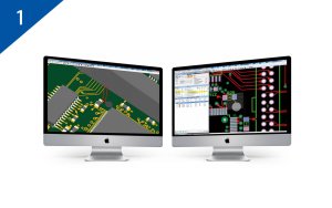
1.1 PCB Design Support Services
Schematic Design
- Translates electronic circuit functional requirements into standardized schematic diagrams
- Ensures correct electrical connection logic, laying the foundation for subsequent PCB layout
PCB Layout Design
- Component placement and signal routing planning based on schematics
- Optimizes high-speed signal paths to reduce EMI
- Strategically plans power and ground planes to ensure power integrity (PI)
1.2 PCB Substrate and Material Selection
Material Comparison Table:
FR-4 High cost-performance ratio, stable electrical properties; suitable for consumer electronics, industrial control;
CEM-1/CEM-3 Lower cost, good processability Suitable for single-sided boards, low-end products;
High-Frequency Materials Low dielectric loss, excellent high-frequency characteristics 5G communications, radar systems;
Aluminum Substrates Superior thermal dissipation Suitable for LED lighting, power modules;
Copper Foil Thickness Selection Criteria:
- Standard signal traces: 1oz (35μm)
- High-current paths: 2oz (70μm) or thicker
- Power/ground planes: Customized based on current-carrying requirements
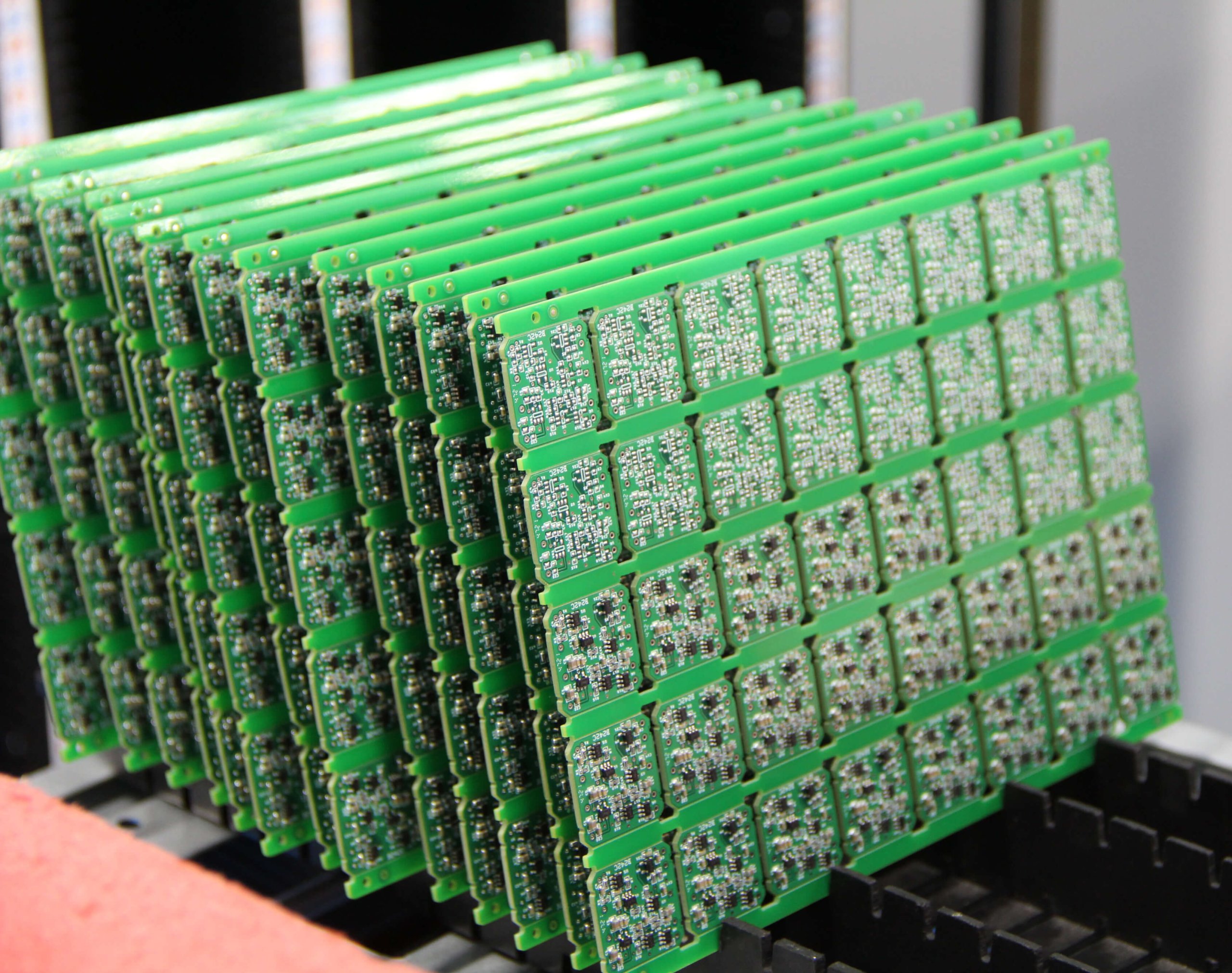
1.3 Core Manufacturing Processes
Photolithography
- Forms precise circuit patterns on substrates via exposure and development
- Line width/spacing achievable below 3mil/3mil (0.075mm)
Etching
- Chemically removes excess copper layers to form precise traces
- Controlled etching factors ensure line width accuracy
Drilling Process
- Mechanical drilling: Hole diameters 0.2mm–6.35mm
- Laser drilling: For micro-holes (<0.15mm) and blind/buried vias
- Hole position accuracy controlled within ±0.05mm
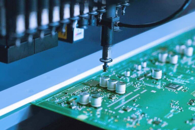
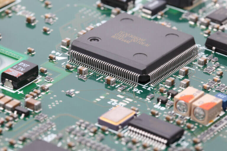
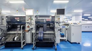
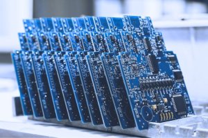
1.4 PCB Assembly Services (PCBA)

SMT Assembly (Surface Mount Technology)
- High-precision placement machines handle components down to 01005 package size
- Optimized reflow soldering temperature profiles ensure reliable connections
THT Assembly (Through-Hole Technology)
- Suitable for high-power devices, connectors, and high-reliability components
- Wave soldering or selective wave soldering processes
Mixed Assembly
- Combines SMT and THT processes to meet complex product requirements
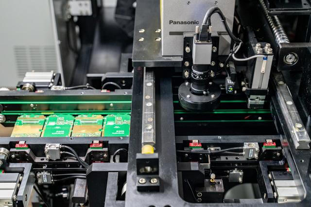
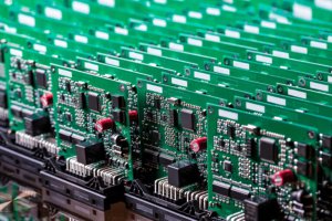
1.5 Quality Inspection and Testing
AOI (Automated Optical Inspection)
- Detects solder joint defects, missing components, and polarity errors
- Detection accuracy: 01005 components and larger
X-Ray Inspection
- Detects internal defects in hidden solder joints (BGA, QFN, etc.)
- Identifies voids, bridging, cold solder joints, etc.
ICT In-Circuit Testing / FCT Functional Testing
- ICT: Detects open circuits, short circuits, and component parameter deviations
- FCT: Verifies overall PCBA functionality against design specifications
1.6 Post-Processing and Protection
Cleaning Process
- Removes flux residues and ionic contaminants
- Meets IPC-A-610 cleanliness standards
Conformal Coating
- Provides moisture, dust, and corrosion protection
- Material options: acrylic, polyurethane, silicone, UV-curable
2. Key Considerations for PCB Manufacturing
2.1 Design Phase: DFM (Design for Manufacturability)
Core Principles:
- Line width/spacing ≥ process capability (typically ≥3mil)
- Maintain hole diameter to board thickness ratio (Aspect Ratio) within reasonable limits
- Reserve process margins and alignment holes for production positioning
- Avoid design hazards like isolated copper pads and sharp-angled traces
Signal Integrity (SI) Assurance:
- Control impedance matching for high-speed signal lines (50Ω/90Ω/100Ω)
- Strictly maintain differential pair length matching with <5mil tolerance
- Avoid crossing partition planes to minimize signal return paths
2.2 Material Selection Compliance
Environmental Standards Compliance:
- RoHS Directive: Restricts hazardous substances like lead, mercury, cadmium
- REACH Regulation: Controls Substances of Very High Concern (SVHC)
- Halogen-free requirement: Suitable for environmentally sensitive markets
Material Property Matching:
- Tg (Glass Transition Temperature): Standard 130°C, ≥150°C recommended for lead-free processes
- Matched CTE (Coefficient of Thermal Expansion) to prevent thermal cycling failure
2.3 Manufacturing Process Control
Environmental Control:
- Cleanroom: Class 10,000 or Class 100,000 cleanliness
- Temperature/Humidity Control: 22±2°C, 50±10% RH
- ESD Protection: Continuous static dissipation and grounding throughout
Batch Traceability Management:
- Unique PCB identification per batch (QR code/barcode)
- Raw material batch records for quality traceability
- Production data logging (temperature profiles, test parameters)
2.4 Comprehensive Quality Inspection System
Incoming Quality Control (IQC): Substrate, copper foil, chemical inspections
In-Process Quality Control (IPQC): First article inspection, patrol inspection, critical process monitoring
Final Quality Control (FQC/OQC): Visual inspection, dimensional measurement, electrical testing
Reliability Testing (as required):
- Thermal Shock Testing
- Humidity and Temperature Stress Testing (HAST)
- Mechanical Vibration/Shock Testing
2.5 Supply Chain and Customer Collaboration
Requirement Confirmation Checklist:
- Specify layer count, board thickness, copper thickness, surface finish process
- Confirm impedance control requirements and test methods
- Define acceptance criteria (IPC-A-600 / IPC-A-610 grade)
Transparent Progress Management:
- Provide production schedules and critical milestone updates
- 24-hour response mechanism for anomalies
- Deliver comprehensive Certificate of Analysis (COA)
3. How to Select a Premium PCB Fabrication Service Provider?
Evaluation Criteria:
- Process Capabilities: Minimum line width/spacing, maximum layer count, specialized processes (HDI, rigid-flex)
- Quality Systems: ISO 9001, IATF 16949 (Automotive), ISO 13485 (Medical) certifications
- Delivery Capability: Prototyping lead time (24-72 hours), on-time delivery rate for volume production
- Industry Experience: Alignment with target sectors (Communications, Medical, Automotive Electronics, Industrial Control)
PCB manufacturing is a precision service involving multi-process coordination. From design support and material selection to precision fabrication and quality inspection, each stage directly impacts final product performance. By adhering to DFM principles, implementing strict material control, maintaining robust quality systems, and ensuring efficient customer communication, we guarantee PCB products meet high reliability standards, empowering electronic devices to excel in competitive markets.