

Demystifying the Acronyms in Electronics Assembly
In the intricate world of electronics manufacturing, acronyms are ubiquitous. Among the most common, and often confused, are CCA and PCBA. While frequently used interchangeably in casual industry dialogue, a professional understanding reveals subtle yet significant distinctions that influence everything from design and manufacturing to quality control and project management. At their core, both terms refer to the fundamental process of populating a bare Printed Circuit Board (PCB) with electronic components to create a functional circuit.
The primary difference lies in terminology and the formal standards that govern them. Circuit Card Assembly (CCA) is the formal term, officially recognized and utilized by industry standards bodies like IPC (Association Connecting Electronics Industries). It is the language of specifications and official documentation. In contrast, Printed Circuit Board Assembly (PCBA)—and its close relative, Printed Circuit Assembly (PCA)—is the more prevalent, informal term used in daily communication by engineers, manufacturers, and designers.
The Core Distinction: Scope, Focus, and Practical Implications
The true divergence between CCA and PCBA is not in the physical act of assembly but in the conceptual boundary of the process. It is a distinction between a component and a system, a part and a whole. This difference in perspective has profound practical implications throughout a product’s lifecycle.
Scope and Focus: The Micro vs. The Macro
The most effective way to understand the difference is to view it through the lens of scope.
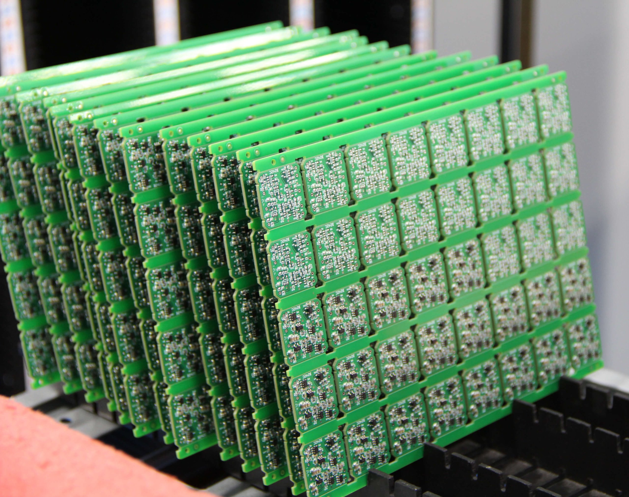
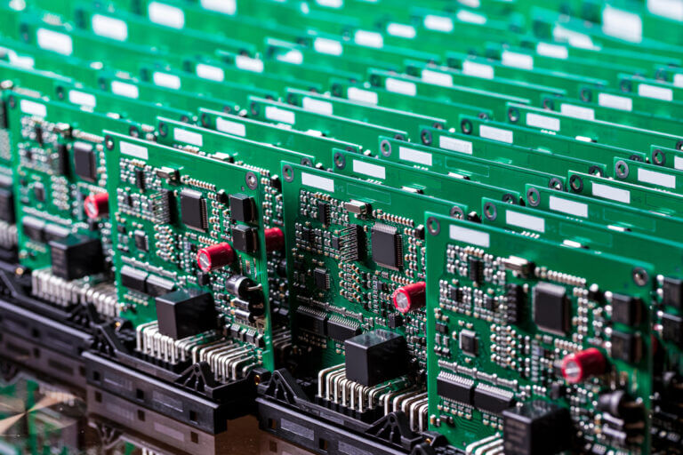
- CCA (The Populated Board): This term focuses narrowly on the board-level assembly. A CCA is the tangible product that comes off the SMT or THT assembly line—a bare PCB that has been populated with all its specified electronic components. Its scope is confined to the physical edges of the board itself. It is a completed component, ready for the next stage.
- PCBA (The Holistic System): This term represents a broader, more holistic perspective. PCBA is best understood as a superset of CCA, encompassing the entire process that transforms the populated board into a fully integrated electronic system ready for its end-use application.
The “beyond CCA” processes that fall under the comprehensive umbrella of PCBA often include:
- Conformal Coating or Potting: Application of protective materials to shield the CCA from moisture, dust, chemicals, and vibration.
- Integration into an Enclosure: Mounting the CCA into its final housing or chassis.
- Cable and Wire Harness Assembly: Connecting the CCA to other system components, power supplies, and user interfaces.
- “Box Build” Assembly: The complete assembly of the final product, which includes the PCBA, enclosure, power supply, displays, and any other mechanical or electronic parts.
- System-Level Testing: Comprehensive testing of the fully assembled product to ensure it functions correctly as a complete system.
Implications for Project Lifecycle
This difference in scope directly impacts key stages of product development:
- Design: A CCA-centric design approach prioritizes optimizing the PCB layout for component density, signal integrity, and manufacturability. A PCBA-centric approach incorporates these factors but also considers mechanical fit within an enclosure, thermal management of the entire system, cable routing, and serviceability.
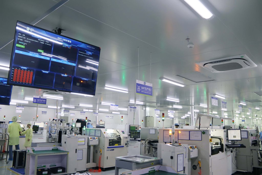
- Manufacturing: CCA manufacturing is defined by core assembly processes like SMT and THT. PCBA manufacturing may involve these plus additional, distinct production lines for mechanical assembly, conformal coating, wire harness fabrication, and final product integration.
- Testing: CCA testing is board-centric, focusing on verifying the integrity of the populated board through methods like Automated Optical Inspection (AOI) and In-Circuit Testing (ICT). PCBA testing expands to include system-level validation, environmental stress screening (ESS), electromagnetic compatibility (EMC) testing, and final quality assurance on the complete, boxed product.
Illustrative Case Studies
Two examples clearly illustrate this practical difference:
Case Study 1: A Simple Digital Thermometer. In this device, the core functionality is delivered by a single board containing a microcontroller, sensor, and display. The CCA is, for all practical purposes, the final product, with only a simple plastic case added. Here, the distinction between CCA and PCBA is minimal, and the project’s focus is almost entirely on the design and assembly of the CCA itself.
Case Study 2: An Industrial Control Unit. This system is far more complex, consisting of multiple CCAs (e.g., a main processor board, a power management board, I/O boards) housed within a ruggedized metal enclosure. These boards are interconnected by a complex wire harness and must operate reliably in a high-vibration, high-temperature environment. In this scenario, a holistic PCBA approach is critical for success. While the quality of each individual CCA is vital, factors like enclosure design, system-level thermal dynamics, cable management, and rigorous system testing are paramount .
The Manufacturing Process: From Bare Board to Functional Unit
Phase 1: Foundation and Preparation
Regardless of the terminology used, the creation of a functional electronic assembly follows a highly controlled and technologically advanced sequence of steps. This process transforms a bare board and a collection of individual components into a cohesive, functional unit.
The process begins long before any components are placed. The foundation must be perfect.
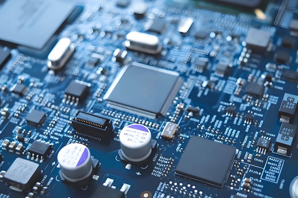
- PCB Fabrication: The journey starts with the fabrication of the bare PCB. A substrate material, most commonly FR-4 (a flame-retardant fiberglass epoxy composite), is layered with copper. Through a process of photolithography and etching, the unwanted copper is removed, leaving behind the intricate network of conductive traces, pads, and planes that form the circuit . Holes are then drilled for component leads or vias.
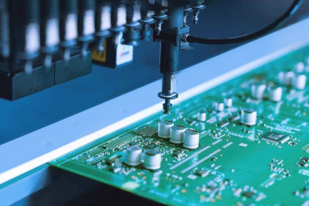
- Solder Paste Application: For surface-mount assembly, a precise amount of solder paste—a mixture of tiny solder spheres and flux—is applied to the component pads on the board. This is typically done using a solder stencil, a thin sheet of metal with laser-cut openings that align perfectly with the pads, ensuring the paste is deposited only where needed.
Phase 2: Component Mounting Technologies
With the board prepared, components are mounted using highly specialized technologies. The choice of technology depends on component type, density requirements, and mechanical stress considerations.
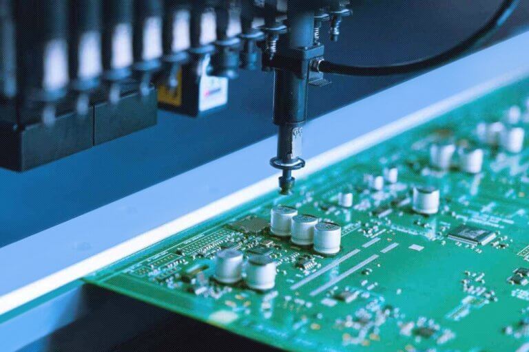
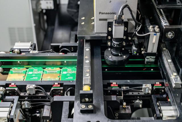
- Surface Mount Technology (SMT): The dominant method in modern electronics. Components designed for SMT, known as Surface Mount Devices (SMDs), have no leads and are placed directly onto the surface of the PCB. This process is highly automated using “pick-and-place” machines that can position thousands of components per hour with extreme precision. SMT allows for higher component density, smaller board sizes, and better high-frequency performance.
- Through-Hole Technology (THT): The traditional assembly method. Components have wire leads that are inserted through holes drilled in the PCB and then soldered to pads on the opposite side. While less dense than SMT, THT provides superior mechanical strength, making it ideal for larger components, connectors, and parts that will undergo mechanical stress .
- Ball Grid Array (BGA): A specialized type of surface-mount packaging used for high-pin-count components like microprocessors and FPGAs. Instead of leads, BGAs use a grid of solder balls on their underside for electrical connection. This allows for a very high number of interconnections in a small footprint but presents challenges for inspection, as the solder joints are hidden beneath the component.
Phase 3: Soldering and Finalization
Once components are in place, the connections must be made permanent.
- Reflow Soldering: Used for SMT assemblies. The board is passed through a long reflow oven with multiple temperature zones. It is gradually heated to activate the flux and melt the solder paste. As the board moves into cooler zones, the solder solidifies, creating strong and reliable electrical connections for all surface-mount components simultaneously .
- Wave Soldering: The primary method for THT components. The board passes over a wave of molten solder, which wicks up into the through-holes and solders the component leads to the board.
- Cleaning and Coating: After soldering, the board is cleaned to remove any flux residues, which can be corrosive or interfere with electrical performance. For applications in harsh environments, a protective conformal coating or a thicker potting compound may be applied to protect the assembly from external factors.
Phase 4: Quality Assurance and Testing
Rigorous inspection and testing are non-negotiable to ensure quality and reliability.
- Automated Optical Inspection (AOI): High-resolution cameras scan the board and compare it to the design files to detect visual defects such as missing or incorrect components, poor solder joints, and incorrect polarity. It is a fast and effective method for catching common manufacturing errors .
- X-Ray Inspection (AXI): Essential for inspecting solder joints that are not visible to the naked eye or AOI cameras, particularly the solder balls under BGA components. AXI can detect voids, shorts, and incomplete connections hidden beneath the chip package.
- In-Circuit Testing (ICT): This test uses a “bed-of-nails” fixture with probes that make contact with test points on the board. ICT powers up the board and checks for shorts, opens, and verifies that individual components (resistors, capacitors, etc.) have the correct values, effectively testing the integrity of the assembly .
- Functional Testing (FCT): The final step in board-level testing. The CCA/PCBA is powered up and its functionality is tested against its design specifications, often by simulating its real-world operating environment. This confirms that the board not only is assembled correctly but also performs as intended.
Key Applications Across Industries
The distinction between a CCA-centric and a PCBA-centric approach becomes clearer when examining the demands of different industries. The required level of integration, reliability, and testing dictates the necessary scope.
- Consumer Electronics (Smartphones, Laptops): This sector is driven by miniaturization, high component density, and cost-effective, high-volume production. The focus is often on producing flawless CCAs at massive scale. While the final product is a full PCBA, the core manufacturing challenge lies in the SMT-heavy CCA.
- Automotive and Industrial (Control Systems, ADAS): Reliability and durability are paramount. These applications often use a mix of SMT for processing power and robust THT components for connectors and high-stress parts. The full PCBA scope is critical, as assemblies must be protected in rugged enclosures and undergo extensive system-level testing to withstand harsh conditions like vibration and temperature extremes .
- Medical Devices (Monitors, Diagnostic Equipment): This industry is governed by stringent regulatory standards like ISO 13485. Flawless execution and complete traceability are required. The process is inherently PCBA-centric, demanding meticulous documentation from the individual CCA through to the final, validated, and sterilized medical device where failure is not an option .
- Aerospace & Defense (Avionics, Satellites): These are among the most demanding applications. A comprehensive PCBA approach is mandatory, focusing on high-reliability (Hi-Rel) materials, resistance to extreme temperatures, radiation, and vacuum. Extensive system-level environmental stress screening (ESS) is performed on the complete PCBA to ensure it can survive and function in its intended hostile environment .
Conclusion
In the lexicon of electronics manufacturing, CCA and PCBA are two terms for the same fundamental action, yet they represent vastly different perspectives. While they are often used interchangeably without consequence in casual conversation, understanding the nuanced difference between the board-level product (CCA) and the holistic system process (PCBA) is a hallmark of a seasoned electronics professional.
This distinction is far from academic. It carries direct consequences for design strategies, manufacturing workflows, testing protocols, and ultimately, project cost and product reliability. A project focused solely on delivering a CCA may overlook critical system-level integration challenges, while a comprehensive PCBA approach ensures that the final product is robust, reliable, and ready for its real-world application.
Ultimately, clarity in communication with design teams, contract manufacturers, and all project stakeholders is paramount. Specifying requirements with a clear understanding of whether the deliverable is a populated board or a fully assembled and tested system ensures alignment, prevents costly misunderstandings, and paves the way for a successful product launch.