
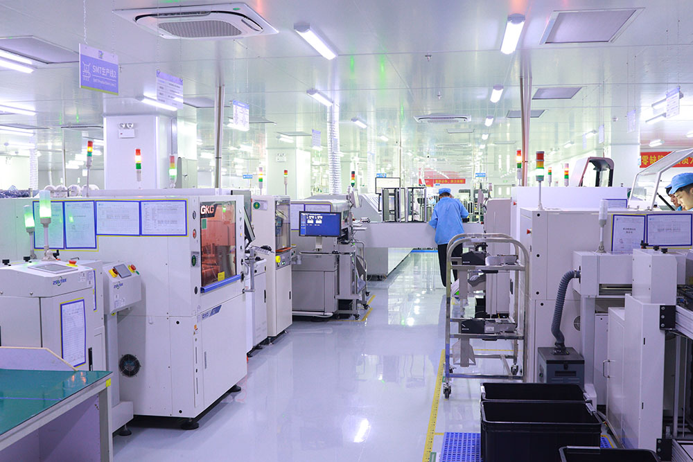
Not every chip lives inside a molded package. In cost-sensitive and space-critical products, the silicon die is mounted directly onto the board and connected with tiny wires. Wire bonding and chip-on-board assembly is the packaging technique behind COB LED modules, low-cost sensors, and ultra-compact electronics where the conventional package would add unacceptable height or expense to the final product.
By skipping the traditional package, COB reduces height, saves material, and shortens electrical paths that would otherwise introduce parasitics and signal loss. The trade-off is that the bare die is fragile and demands a clean, controlled assembly environment with discipline that standard SMT lines may not provide by default without added controls.
The Die Attach Step
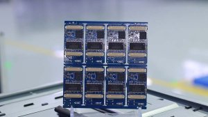
Assembly begins by attaching the die to the board with adhesive or solder. Epoxy provides mechanical strength and electrical insulation for the die back, while conductive paste or solder creates a thermal and ground path for devices that need to shed heat through the substrate. The choice depends on whether the die back is grounded, floating, or thermally critical to reliability.
Placement accuracy is critical: the die must land within microns of its target so the bond pads align with the substrate fingers. Vision-guided die bonders achieve this repeatedly, then cure the attach material under controlled temperature and time to develop full adhesion without stressing the silicon or shifting the placement during the cure cycle.
Wire Bonding Fundamentals
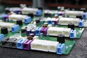
Once attached, the die is connected by ultrasonically bonding fine wires, usually gold or copper, between the chip pads and the board. The process uses heat, pressure, and vibration to fuse the wire to the metal surfaces without damaging the delicate die or its thin bond pads, and it is repeated for every connection on the device in a programmed sequence.
Gold wire remains popular for its reliability and ease of bonding, while copper offers lower cost and better electrical and thermal performance at the expense of stricter process control and faster oxidation management. A specialist PCB assembly manufacturer selects the wire based on the product’s reliability requirements, operating environment, and budget, and validates the bond schedule on actual parts before committing to volume.
Ball and Wedge Bonds
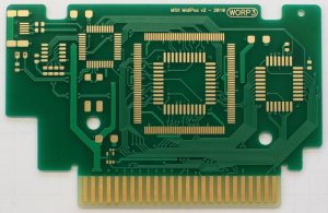
Gold wire typically forms a ball bond on the die and a wedge bond on the substrate, whereas copper and aluminum often use wedge-to-wedge bonding. Each style has characteristic shapes visible under inspection and different sensitivities to contamination, and the loop height of the wire affects both stress and clearance to the eventual encapsulant that will cover it.
Encapsulation and Protection
Bare wires are vulnerable to mechanical and environmental damage, so COB assemblies are usually encapsulated. A dome of epoxy or silicone covers the die and wires, protecting them from moisture, vibration, and handling while also acting as a lens in LED modules to shape the emitted light into the intended pattern.
The encapsulant must match the die and substrate thermally and chemically. A mismatch causes delamination or stress cracks that fail in the field, which is why a careful one-stop PCBA solution validates the material through temperature cycling and humidity testing before committing to production volumes that would be expensive to recall.
COB vs Traditional Packaging
Compared with surface-mount packaged parts, COB removes the package body and its associated height, cost, and parasitic inductance. For LED modules this yields a continuous emitting surface impossible with discrete packages, and for sensors it shortens signal paths that improve noise performance. The downside is testability: a bare die cannot be pre-tested as easily as a packaged part, shifting more validation onto the assembled module.
This trade makes COB ideal where those disadvantages are manageable, such as mature, high-volume designs whose die is already well characterized. For early prototypes or low volumes, packaged parts may be the safer and faster route until the design is frozen and the volume justifies the COB investment.
Where COB Delivers Value
COB shines where package height, cost per unit, or optical performance dominate. LED light engines use it to create uniform emitting surfaces, and many consumer modules use it to trim pennies across million-unit runs where package cost is a large fraction of total bill of materials and even small savings are strategic.
The approach is less suited to products needing easy chip replacement or harsh-environment robustness without heavy encapsulation. Designers weigh these factors against the savings COB provides, and increasingly choose it as automated bonding equipment makes the process more repeatable and less dependent on operator skill.
Quality Assurance for Bare Die
Because defects are invisible without magnification, COB lines rely on bond-pull testing, shear testing, and microscopic inspection at frequency. Monitoring bond strength and ball size over time catches process drift before it reaches the customer, and statistical control of the bond parameters keeps yield stable across long production runs rather than only at startup.
Mastered correctly, chip-on-board assembly delivers packaging performance that molded packages cannot match, at a fraction of the footprint and cost. It remains a cornerstone of advanced, miniaturized, and cost-driven electronics, and a differentiating capability for manufacturers who can deliver it reliably.
